

Fairchild Semiconductor 74LVQ241SC, 74LVQ241QSCX, 74LVQ241QSC, 74LVQ241MSAX, 74LVQ241MSA Datasheet
...
74LVQ241
Low Voltage Octal Buffer/Line Driver with 3-STATE
Outputs
General Description
The LVQ241isanoctalbufferandlinedriverdesignedtobe
employed as a memory address driver, clock driver and bus
oriented transmitter or receiver which provides improved PC
board density.
Features
n Ideal for low power/low noise 3.3V applications
n Implements patented EMI reduction circuitry
n Available in SOIC JEDEC, SOIC EIAJ and QSOP
packages
n Guaranteed simultaneous switching noise level and
dynamic threshold performance
n Improved latch-up immunity
n Guaranteed incident wave switching into 75Ω
n 4 kV minimum ESD immunity
Ordering Code:
Order Number Package Number Package Description
74LVQ241SC M20B 20-Lead (0.300" Wide) Molded Small Outline Package, SOIC JEDEC
74LVQ241SJ M20D 20-Lead Molded Shrink Small Outline Package, SOIC EIAJ
74LVQ241QSC MQA20 20-Lead (0.150" Wide) Molded Shrink Small Outline Package, SSOP JEDEC
Device also available in Tape and Reel. Specify by appending suffix letter “X” to the ordering code.
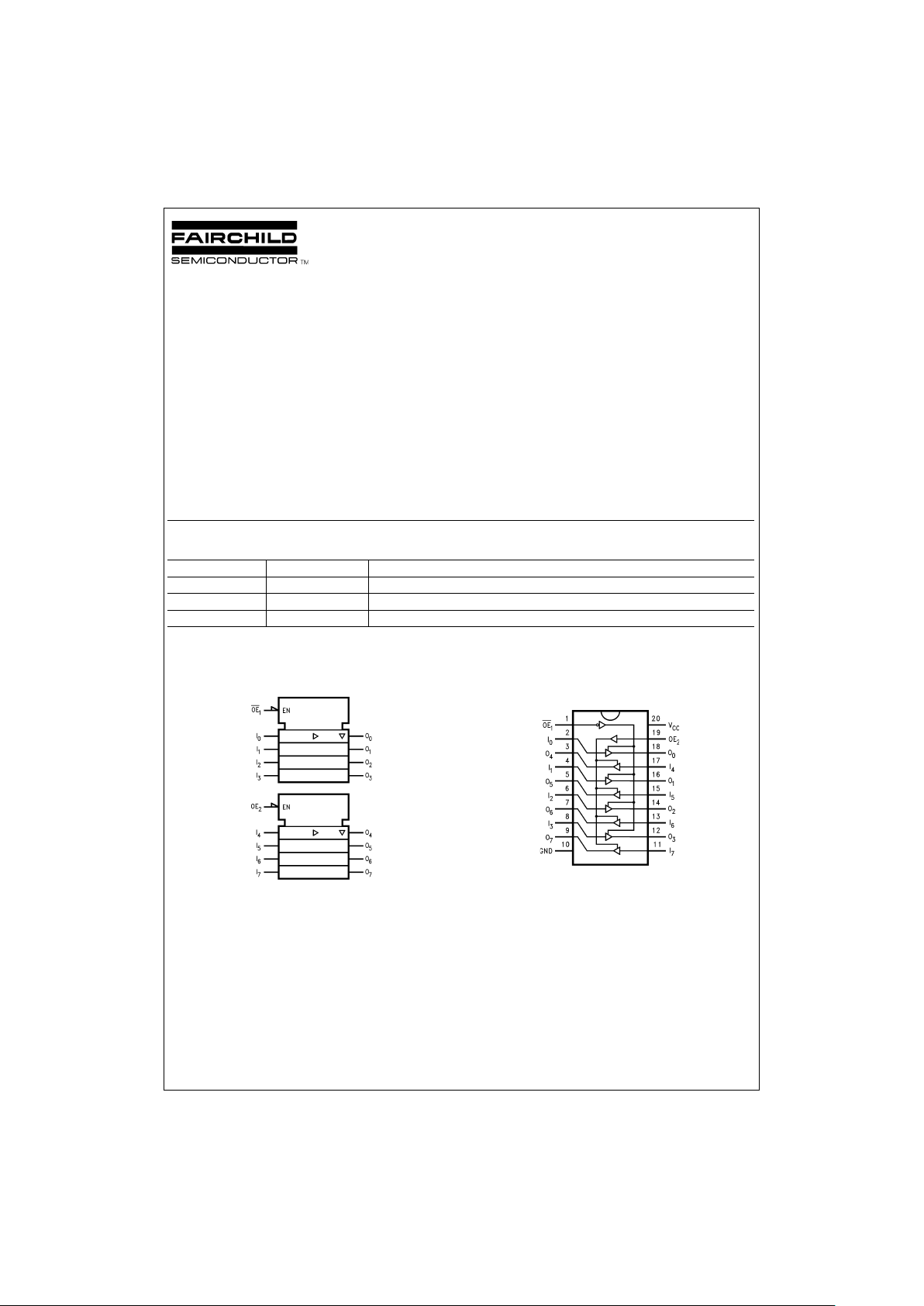
Logic Symbol Connection Diagram
IEEE/IEC
DS011355-1
Pin Assignment for
SOIC andQSOP
DS011355-2
April 1998
74LVQ241 Low Voltage Octal Buffer/Line Driver with 3-STATE Outputs
© 1998 Fairchild Semiconductor Corporation DS011355 www.fairchildsemi.com
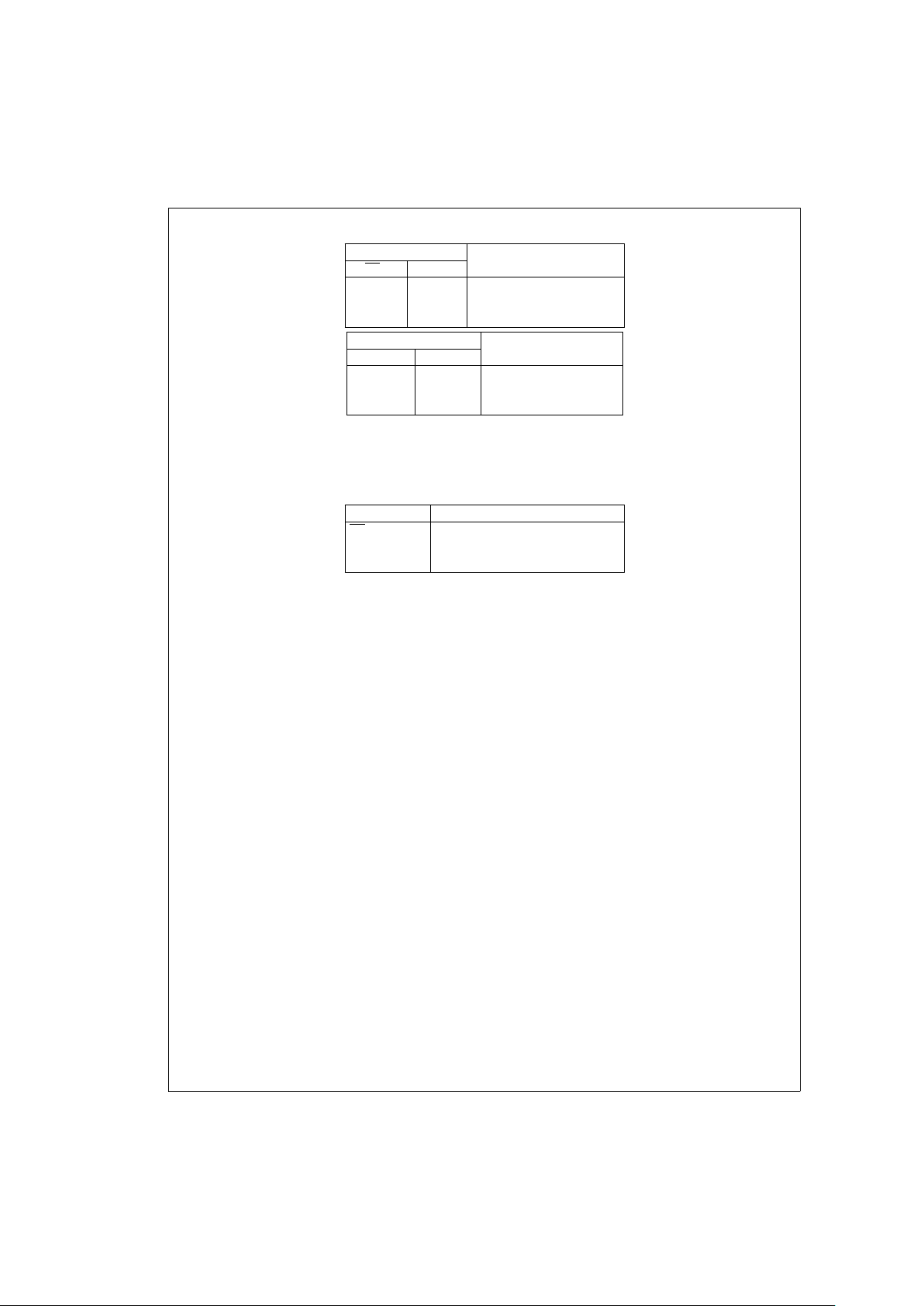
Truth Tables
Inputs Outputs
OE
1
I
n
(Pins 12, 14, 16, 18)
LL L
LH H
HX Z
Inputs Outputs
OE
2
I
n
(Pins 3, 5, 7, 9)
LX Z
HH H
HL L
H
=
HIGH Voltage Level
X=Immaterial
L=LOW Voltage Level
Z=High Impedance
Pin Descriptions
Pin Names Description
OE
1
,OE
2
3-STATE Output Enable Inputs
I
0–I7
Inputs
O
0–O7
Outputs
www.fairchildsemi.com 2
 Loading...