


Fairchild Semiconductor 74LVQ240QSCX, 74LVQ240QSC, 74LVQ240SJX, 74LVQ240SJ, 74LVQ240SCX Datasheet
...
74LVQ240
Low Voltage Octal Buffer/Line Driver with 3-STATE
Outputs
General Description
The LVQ240 is an inverting octal buffer and line driver designed to be employed as a memory address driver, clock
driver and bus oriented transmitter or receiver which provides improved PC board density.
Features
n Ideal for low power/low noise 3.3V applications
n Implements patented EMI reduction circuitry
n Available in SOIC JEDEC, SOIC EIAJ, and QSOP
packages
n Guaranteed simultaneous switching noise level and
dynamic threshold performance
n Improved latch-up immunity
n Guaranteed incident wave switching into 75Ω
n 4 kV minimum ESD immunity
Ordering Code:
Order Number Package Number Package Description
74LVQ240SC M20B 20-Lead (0.300" Wide) Molded Small Outline Package, SOIC, JEDEC
74LVQ240SJ M20D 20-Lead Molded Shrink Small Outline Package, SOIC, EIAJ
74LVQ240QSC MQA20 20-Lead (0.150" Wide) Molded Shrink Small Outline Package, SSOP, JEDEC
Devices also available in Tape and Reel. Specify by appending suffix letter “X” to the ordering code.
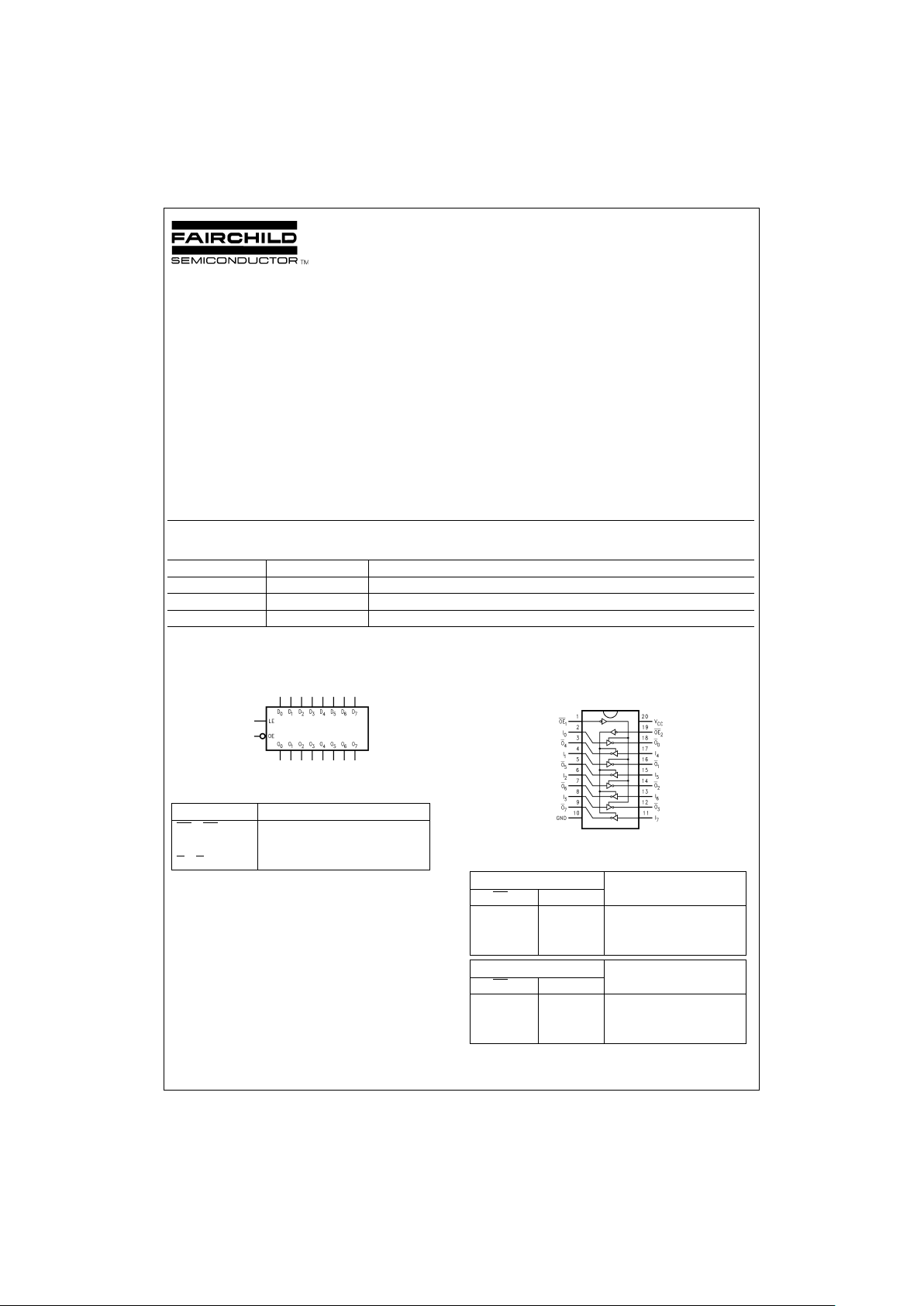
Logic Symbol
Pin Descriptions
Pin Names Description
OE
1
,OE
2
3-STATE Output Enable Inputs
I
0–I7
Inputs
O
0–O7
Outputs
Connection Diagram
Truth Tables
Inputs Outputs
OE
1
I
n
(Pins 12, 14, 16, 18)
LL H
LH L
HX Z
Inputs Outputs
OE
2
I
n
(Pins 3, 5, 7, 9)
LL H
LH L
HX Z
H
=
HIGH Voltage Level L=LOW Voltage Level
X=Immaterial Z=High Impedance
IEEE/IEC
DS011611-1
Pin Assignment,
SOIC and QSOP
DS011611-2
May 1998
74LVQ240 Low Voltage Octal Buffer/Line Driver with 3-STATE Outputs
© 1998 Fairchild Semiconductor Corporation DS011611 www.fairchildsemi.com
Absolute Maximum Ratings (Note 1)
Supply Voltage (V
CC
) −0.5V to +7.0V
DC Input Diode Current (I
IK
)
V
I
=
−0.5V −20 mA
V
I
=
V
CC
+ 0.5V +20 mA
DC Input Voltage (V
I
) −0.5V to VCC+ 0.5V
DC Output Diode Current (I
OK
)
V
O
=
−0.5V −20 mA
V
O
=
V
CC
+ 0.5V +20 mA
DC Output Voltage (V
O
) −0.5V to VCC+ 0.5V
DC Output Source
or Sink Current (I
O
)
±
50 mA
DC V
CC
or Ground Current
(I
CC
or I
GND
)
±
400 mA
Storage Temperature (T
STG
) −65˚C to +150˚C
DC Latch-Up Source or
Sink Current
±
300 mA
Recommended Operating
Conditions
(Note 2)
Supply Voltage (V
CC
) 2.0V to 3.6V
Input Voltage (V
I
) 0VtoV
CC
Output Voltage (VO) 0VtoV
CC
Operating Temperature (TA) −40˚C to +85˚C
Minimum Input Edge Rate (∆V/∆t)
V
IN
0.8V to 2.0V
V
CC
@
3.0V 125 mV/ns
Note 1: The “Absolute Maximum Ratings” are those values beyond which
the safety of the device cannot be guaranteed. The device should not be operated at these limits. The parametric values defined in the Electrical Characteristics tables are not guaranteed at the absolute maximum ratings. The
“Recommended Operating Conditions” table will define the conditions for actual device operation.
Note 2: Unused inputs must be held HIGH or LOW. They may not float.
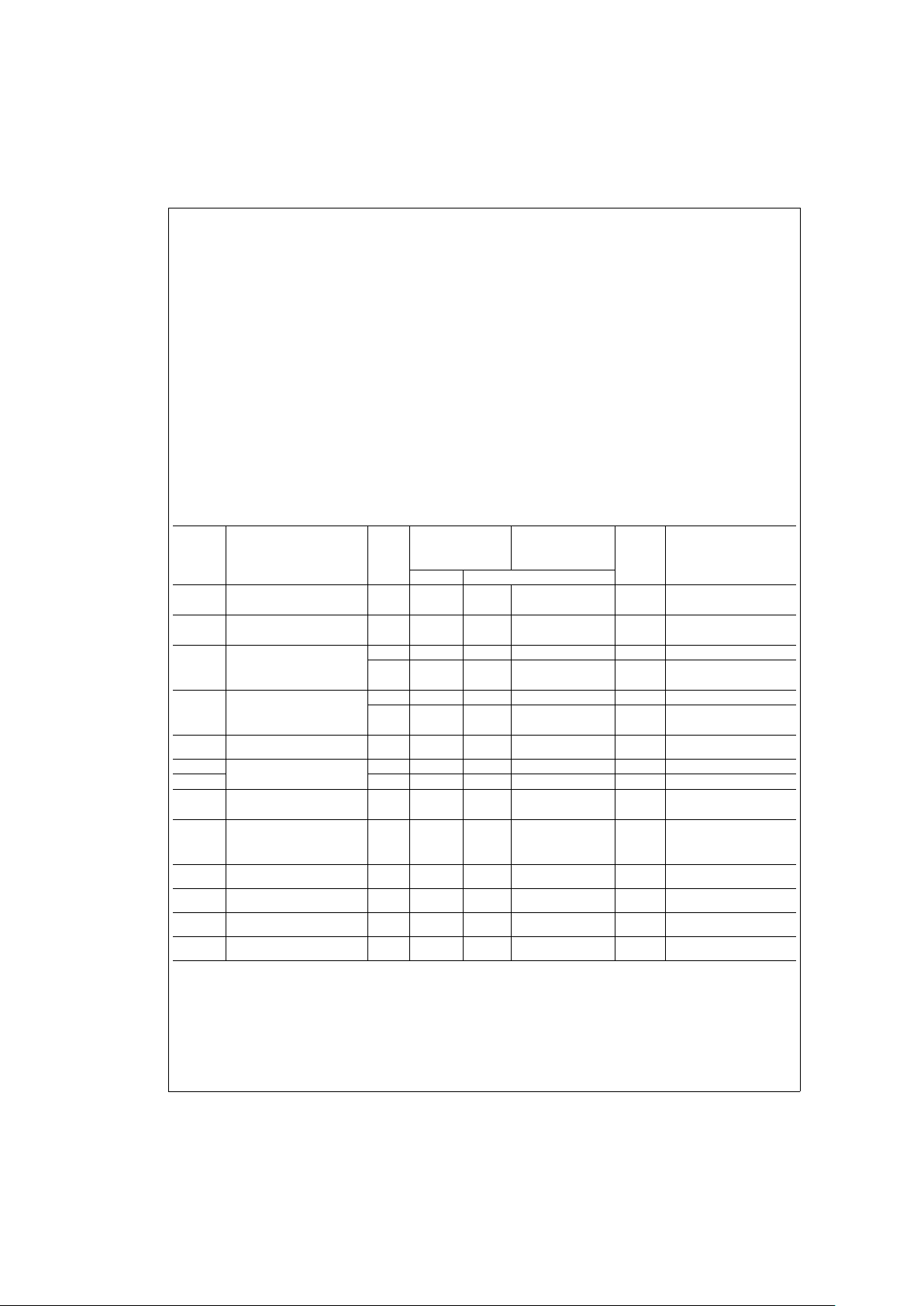
DC Electrical Characteristics
Symbol Parameter
V
CC
(V)
T
A
=
+25˚C T
A
=
−40˚C to +85˚C Units Conditions
Typ Guaranteed Limits
V
IH
Minimum High Level
Input Voltage
3.0 1.5 2.0 2.0 V V
OUT
=
0.1V
or V
CC
− 0.1V
V
IL
Maximum Low Level
Input Voltage
3.0 1.5 0.8 0.8 V V
OUT
=
0.1V
or V
CC
− 0.1V
V
OH
Minimum High Level
Output Voltage
3.0 2.99 2.9 2.9 V I
OUT
=
−50 µA
3.0 2.58 2.48 V V
IN
=
V
IL
or VIH(Note 3)
I
OH
=
−12 mA
V
OL
Maximum Low Level
Output Voltage
3.0 0.002 0.1 0.1 V I
OUT
=
50 µA
3.0 0.36 0.44 V V
IN
=
V
IL
or VIH(Note 3)
I
OL
=
12 mA
I
IN
Maximum Input
Leakage Current
3.6
±
0.1
±
1.0 µA V
I
=
V
CC
, GND
I
OLD
Minimum Dynamic
Output Current (Note 4)
3.6 36 mA V
OLD
=
0.8V Max (Note 5)
I
OHD
3.6 −25 mA V
OHD
=
2.0V Min (Note 5)
I
CC
Maximum Quiescent
Supply Current
3.6 4.0 40.0 µA V
IN
=
V
CC
or GND
I
OZ
Maximum 3-STATE
Leakage Current
3.6
±
0.25
±
2.5 µA VI(OE)=VIL,V
IH
V
I
=
V
CC
, GND
V
O
=
V
CC
, GND
V
OLP
Quiet Output
Maximum Dynamic V
OL
3.3 0.4 0.8 V (Notes 6, 7)
V
OLV
Quiet Output
Minimum Dynamic V
OL
3.3 −0.4 −0.8 V (Notes 6, 7)
V
IHD
Maximum High Level
Dynamic Input Voltage
3.3 1.6 2.0 V (Notes 6, 8)
V
ILD
Maximum Low Level
Dynamic Input Voltage
3.3 1.6 0.8 V (Notes 6, 8)
Note 3: All outputs loaded; thresholds on input associated with output under test.
Note 4: Maximum test duration 2.0 ms, one output loaded at a time.
Note 5: Incident wave switching on transmission lines with impedances as low as 75Ω for commercial temperature range is guaranteed for 74LVQ.
Note 6: Worst case package.
Note 7: Max number of outputs defined as (n). Data Inputs are driven 0V to 3.3V. One output
@
GND.
Note 8: Max number of Data Inputs (n) switching. n−1 Inputs switching 0V to 3.3V. Input-under-test switching: 3.3V to threshold (V
ILD
), 0V to threshold (V
IHD
),
f=1 MHz.
www.fairchildsemi.com 2