

Fairchild Semiconductor 74LVQ174SJX, 74LVQ174SJ, 74LVQ174SCX, 74LVQ174SC Datasheet
74LVQ174
Low Voltage Hex D-Type Flip-Flop with Master Reset
General Description
The LVQ174isahigh-speedhexD-typeflip-flop.Thedevice
is used primarily as a 6-bit edge-triggered storage register.
The information on the Dinputsistransferredto storage during the LOW-to-HIGH clock transition. The device has a
Master Reset to simultaneously clear all flip-flops.
Features
n Ideal for low power/low noise 3.3V applications
n Guaranteed simultaneous switching noise level and
dynamic threshold performance
n Guaranteed pin-to-pin skew AC performance
n Guaranteed incident wave switching into 75Ω
Ordering Code:
Order Number Package Number Package Description
74LVQ174SC M16A 16-Lead (0.150" Wide) Small Outline Integrated Circuit, SOIC JEDEC
74LVQ174SJ M16D 16-Lead Molded Small Outline Package, SOIC EIAJ
Devices also available in Tape and Reel. Specify by appending suffix letter “X” to the ordering code.
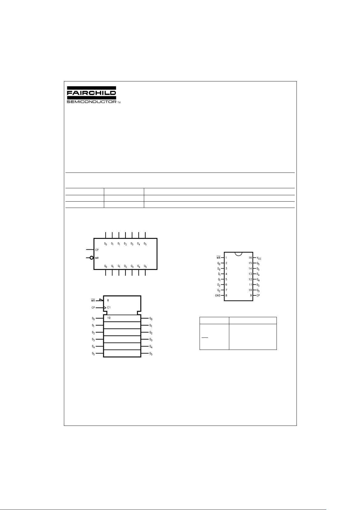
Logic Symbols
Connection Diagram
Pin Descriptions
Pin Names Description
D
0–D5
Data Inputs
CP Clock Pulse Input
MR
Master Reset Input
Q
0–Q5
Outputs
DS011353-1
IEEE/IEC
DS011353-2
Pin Assignment for
SOIC JEDEC and EIAJ
DS011353-3
May 1998
74LVQ174 Low Voltage Hex D-Type Flip-Flop with Master Reset
© 1998 Fairchild Semiconductor Corporation DS011353 www.fairchildsemi.com
Functional Description
The LVQ174 consists of six edge-triggered D flip-flops with
individual D inputs and Q outputs. The Clock (CP) and Master Reset (MR) are common to all flip-flops. Each D input’s
state is transferred to the corresponding flip-flop’s output following the LOW-to-HIGH Clock (CP) transition. A LOW input
to the Master Reset (MR) will force all outputs LOW independent of Clock or Data inputs. The LVQ174 is useful for applications where the true output only is required and the Clock
and Master Reset are common to all storage elements.
Truth Table
Inputs Output
MR
CP D Q
LXX L
H
N
HH
H
N
LL
HLX Q
H=HIGH Voltage Level
L=LOW Voltage Level
X=Immaterial
N
=
LOW-to-HIGH Transition
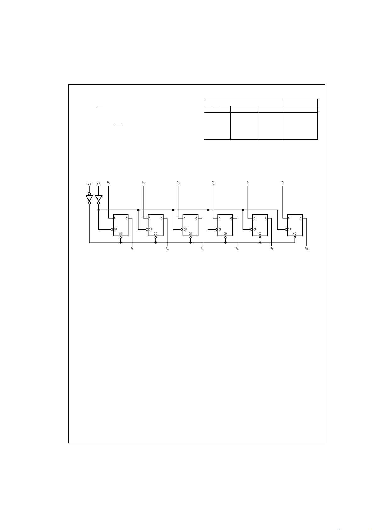
Logic Diagram
DS011353-5
Please note that this diagram is provided only for the understanding of logic operations and should not be used to estimate propagation delays.
www.fairchildsemi.com 2
 Loading...