

Fairchild Semiconductor 74LCXZ245 Datasheet
74LCXZ245
Low Voltage Bidirectional Transceiver
with 5V Tolerant Inputs and Outputs
74LCXZ245 Low Voltage Bidirectional Transceiver with 5V Tolerant Inputs and Outputs
October 2000
Revised October 2000
General Description
The 74LCXZ245 con tains eight non-inverting bidirectional
buffers with 3-STATE outputs and is in tended for bus oriented applications. The device is designed fo r low voltage
(2.5V and 3.3V) V
ing to a 5V signal en vironment. The T /R
the direction of d ata flo w t hro ugh t he de vi ce. T he O E
disables both the A and B ports by placing them in a high
impedance state.
The 74LCXZ245 is fabricated with an advanced CMOS
technology to achieve high speed operation while maintaining CMOS low power dissipation. When V
and 1.5V, the 74LCXZ245 is on the high imped ance state
during power up or pow e r d own. This places the ou tpu ts i n
the high impedance (Z) state preventing intermittent low
impedance loading or glitching in bus oriented applications.
applications with capability of interfac-
CC
input determines
is between 0V
CC
input
Features
■ 5V tolerant inputs and outputs
■ 2.3V–3.6V V
■ 7.0 ns t
■ Power down high impedance inputs and outputs
■ Supports live insertion/withdrawal (Note 1)
■
±24 mA output drive (V
■ Implements patented noise/EMI reduction circuitry
■ Latch-up performance exce eds 500 mA
■ ESD performance:
Human body model
Machine model
Note 1: To ensure the high-impedance state during power up or down, OE
should be tied to VCC through a pull-up res istor: the m inimu m value or t he
resistor is determin ed by the current-sourc ing capability of the driver.
specifications provided
CC
max (V
PD
CC
> 2000V
> 200V
= 3.3V), 10 µA I
= 3.0V)
CC
max
CC
Ordering Code:
Order Number Package Number Package Description
74LCXZ245WM M20B 20-Lead Small Outline Integrated Circuit (SOIC), JEDEC MS-013, 0.300" Wide
74LCXZ245SJ M20D 20-Lead Small Outline Package (SOP), EIAJ TYPE II, 5.3mm Wide
74LCXZ245MSA MSA20 20-Lead Shrink Small Outline Package (SSOP), EIAJ TYPE II, 5.3mm Wide
74LCXZ245MTC MTC20 20-Lead Thin Shrink Small Outline Package (TSSOP), JEDEC MO-153, 4.4mm Wide
Devices also availab l e in Tape and Reel. Specify by appending th e s uffix let t er “X” to the ordering code.
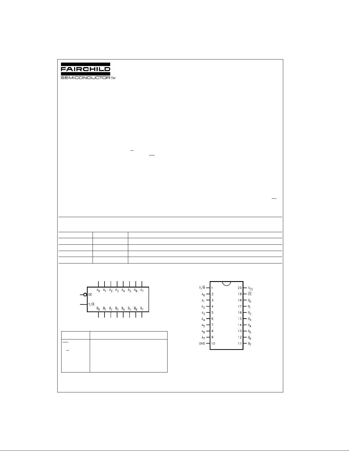
Logic Symbol
Connection Diagram
Pin Descriptions
Pin Names Description
OE
T/R
A
0–A7
B
0–B7
© 2000 Fairchild Semiconductor Corporation DS500362 www.fairchildsemi.com
Output Enable Input
Transmit/Receive Input
Side A Inputs or 3-STATE Outputs
Side B Inputs or 3-STATE Outputs
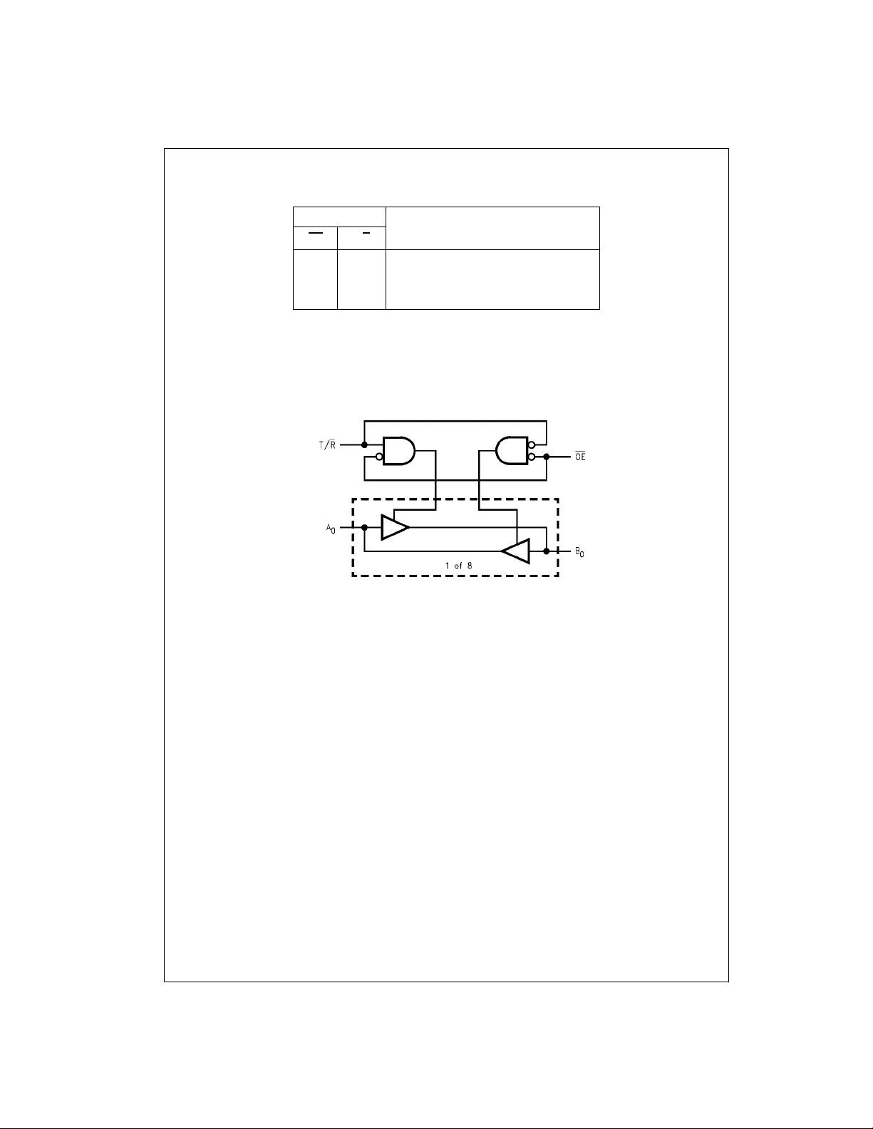
Truth Table
74LCXZ245
H = HIGH Voltage Level
L = LOW Voltage Level
X = Immaterial
Z = High Impedance
Note 2: Unused bus termina ls during HIGH Z State must be held HIGH or LO W.
Inputs
OE
T/R
L L Bus B0 – B7 Data to Bus A0 – A
L H Bus A0 – A7 Data to Bus B0 – B
H X HIGH Z State on A0 – A7, B0 – B7 (Note 2)
Logic Diagram
Outputs
7
7
www.fairchildsemi.com 2
Absolute Maximum Ratings(Note 3)
Symbol Parameter Value Conditions Units
V
V
V
I
IK
I
OK
I
O
I
CC
I
GND
T
CC
I
O
STG
Supply Voltage −0.5 to +7.0 V
DC Input Voltage −0.5 to +7.0 V
DC Output Voltage −0.5 to +7.0 Output in 3-STATE
−0.5 to V
+ 0.5 Output in HIGH or LOW St ate (Note 4)
CC
DC Input Diode Current −50 VI < GND mA
DC Output Diode Current −50 VO < GND
+50 V
O
> V
CC
mA
DC Output Source/Sink Current ±50 mA
DC Supply Current per Supply Pin ±100 mA
DC Ground Current per Ground Pin ±100 mA
Storage Temperature −65 to +150 °C
Recommended Operating Conditions (Note 5)
Symbol Parameter Min Max Units
V
CC
V
I
V
O
I
OH/IOL
T
A
∆t/∆V Input Edge Rate, V
Note 3: The Absolute Maximum Ratings are those values beyond which the safety of the device cannot be guaranteed. The device should not be operated
at these limits. The parametric values defined in the Electrical Characteristics tables are not guaranteed at the Absolute Maximum Ratings. The “Recom-
mended Operating Conditions” table w ill define the conditions fo r ac t ual device operation.
Note 4: I
Note 5: Unused inputs or I/O pins m us t be held HIGH or LOW. They may not float.
Supply Voltage Operating 2.7 3.6 V
Input Voltage 05.5V
Output Voltage HIGH or LOW State 0 V
3-STATE 0 5.5
CC
V
Output Current VCC = 3.0V − 3.6V ±24
= 2.7V - 3.0V ±12
CC
V
= 2.3V - 2.7V ±8
CC
mAV
Free-Air Operating T emperature −40 85 °C
= 0.8V − 2.0V, VCC = 3.0V 0 10 ns/V
IN
Absolute Maximum Rating must be observed.
O
74LCXZ245
V
DC Electrical Characteristics
Symbol Parameter Conditions
V
IH
V
IL
V
OH
V
OL
I
I
I
OZ
I
OFF
I
PU/PD
HIGH Level Input Voltage 2.3 − 2.7 1.7
LOW Level Input Voltage 2.3 − 2.7 0.7
HIGH Level Output Voltage IOH = −100 µA 2.3 - 3.6 VCC − 0.2
LOW Level Output Voltage IOL = 100 µA2.3 − 3.6 0.2
Input Leakage Current 0 ≤ VI ≤ 5.5V 2.3 − 3.6 ±5.0 µA
3-STATE I/O Leakage 0 ≤ VO ≤ 5.5V
Power-Off Leakage Current VI or VO = 5.5V 0 10 µA
Power Up/ Power Down VO = to V
3-STATE Output Current VI = VCC or GND
IOH = −8 mA 2.3 1.8
IOH = −12 mA 2.7 2.2
IOH = −18 mA 3.0 2.4
IOH = −24 mA 3.0 2.2
IOL = 8mA 2.3 0.6
IOL = 12 mA 2.7 0.4
IOL = 16 mA 3.0 0.4
IOL = 24 mA 3.0 0.55
VI = VIH or V
IL
CC
3 www.fairchildsemi.com
V
TA = −40°C to +85°C
CC
(V) Min Max
2.7 − 3.6 2.0
2.7 - 3.6 0.8
2.3 − 3.6 ±5.0 µA
0 − 1.5 ±5.0 µA
Units
V
V
V
V
 Loading...