

Fairchild Semiconductor 74LCXZ16245 Datasheet
74LCXZ16245
Low Voltage 16-Bit Bidirectional Transceiver
with 5V Tolerant Inputs and Outputs
74LCXZ16245 Low Voltage 16-Bit Bidirectional Transceiver with 5V Tolerant Inputs and Outputs
March 2002
Revised March 2002
General Description
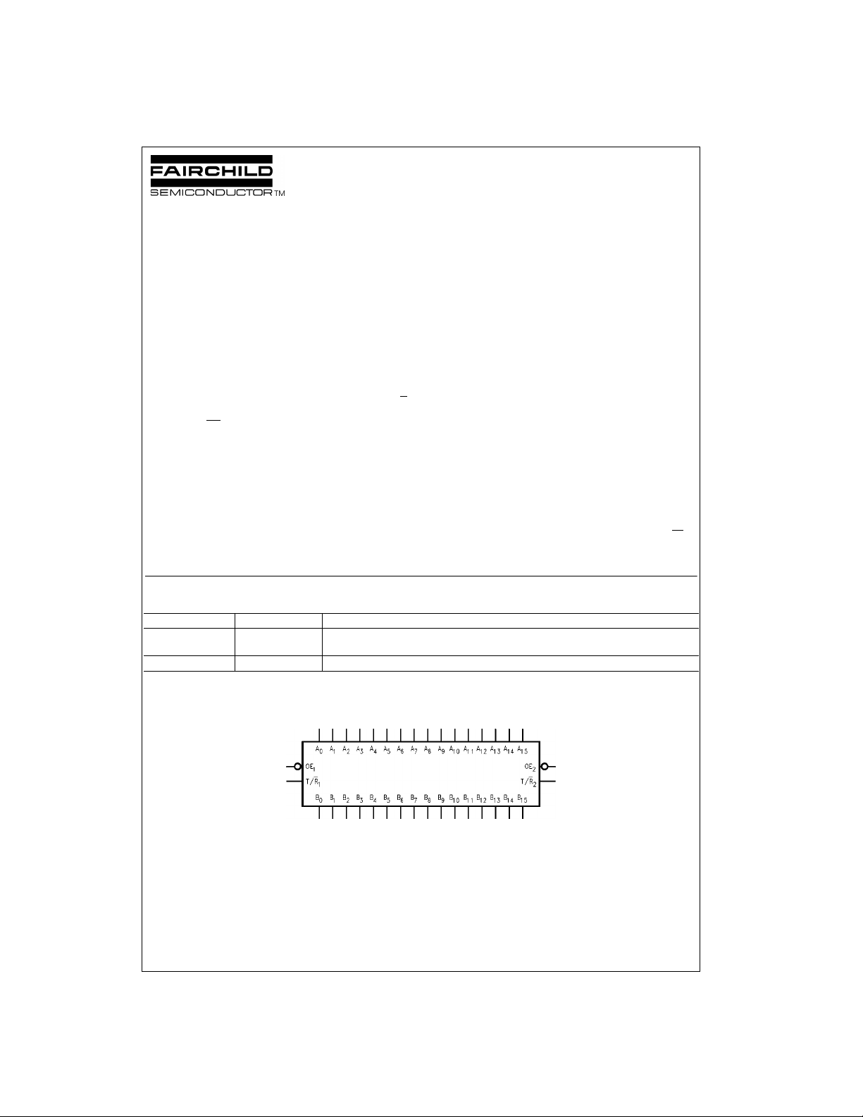
The LCXZ16245 contains sixteen non-inverting bidirectional buffers with 3-STATE outputs and is intended for bus
oriented application s. The device is de signed for low vo ltage (2.7V or 3.3V) V
facing to a 5V signal environment. The device is byte
controlled. Each byte has separate control inputs which
could be shorted toge ther fo r ful l 16-bit op eration . The T /R
inputs determine the direction of data flow through the
device. The OE
placing them in a high impedance state.
When V
the high impedance stat e durin g power- up or po wer -down.
This places the outp uts in the high impedance (Z) state
preventing intermitt ent low impedance loadin g or glitching
in bus oriented applications.
The LCXZ16245 is fabricated with an advanced CMOS
technology to achieve high speed operation while maintaining CMOS low power dissipation.
is between 0V and 1.5V, the LCXZ16245 is on
CC
applications with capability of inter-
CC
inputs disable bo th the A and B ports by
Features
■ 5V tolerant inputs and outputs
■ 2.7V–3.6V V
■ 4.5 ns t
■ Power-down high impedance inputs and outputs
■ Supports live insertion/withdrawal (Note 1)
■
±24 mA output drive (V
■ Implements patented noise/EMI reduction circuitry
■ Latch-up performan ce conforms to the requ irements of
JESD78
■ ESD performance:
Human body model
Machine model
■ Also packaged in plastic Fine-Pitch Ball Grid Array
(FBGA) (Preliminary)
Note 1: To ensure the high-impedance state during power up or down, OE
should be tied to VCC through a pull-up res istor: the m inimu m value or t he
resistor is determin ed by the current-sourc ing capability of the driver.
specifications provided
CC
max (VCC = 3.3V), 20 µA ICC max
PD
= 3.0V)
CC
> 2000V
> 200V
Ordering Code:
Order Number Package Number Package Description
74LCXZ16245GX
(Note 2)
74LCXZ16245MTD MTD48 48-Lead Thin Shrink Small Outline Package (TSSOP), JEDEC MO-153, 6.1mm Wide
Devices also availab l e in Tape and Reel. Specify by appending th e s uffix let t er “X” to the ordering code.
Note 2: BGA package available in Tape and Reel only.
BGA54A
(Preliminary)
54-Ball Fine-Pitch Ball Grid Array (FBGA), JEDEC MO-205, 5.5mm Wide
[TAPE and REEL]
Logic Symbol
© 2002 Fairchild Semiconductor Corporation DS500580 www.fairchildsemi.com
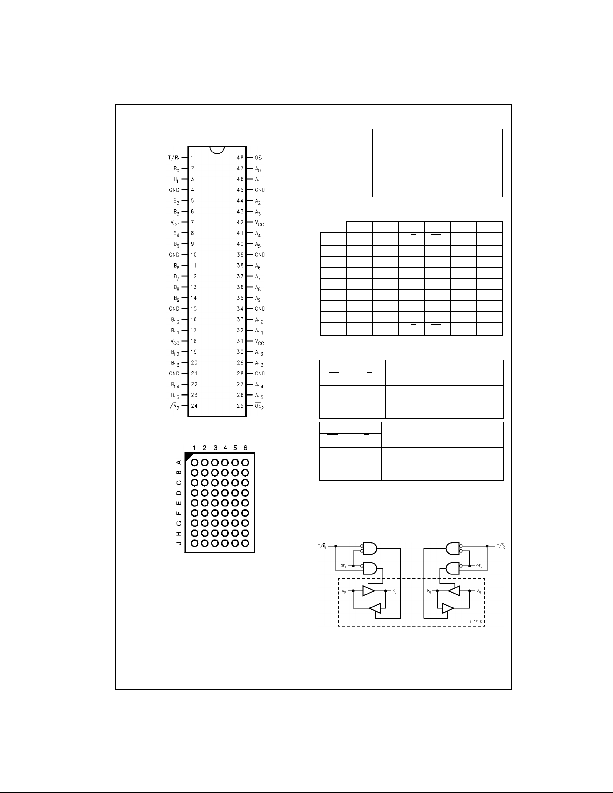
Connection Diagrams
Pin Assignment for SSOP and TSSOP
74LCXZ16245
Pin Assignment for FBGA
Pin Descriptions
Pin Names Description
OE
T/R
A
0–A15
B
0–B15
n
n
Output Enable Input
Transmit/Receive Input
Side A Inputs or 3-STATE Outputs
Side B Inputs or 3-STATE Outputs
NC No Connect
FBGA Pin Assignments
123456
A B
B B
C B
H B
E B
F B
G B
H B
J B
NC T/R1OE1NC A
0
B
2
4
6
8
10
12
14
15
NC NC A
1
B3V
CCVCC
B5GND GND A
B7GND GND A
B9GND GND A9A
B11V
CCVCCA11
B
NC NC A
13
NC T/R2OE2NC A
Truth Ta bles
Inputs
OE
T/R
1
1
LLBus B
LHBus A
H X HIGH Z State on A0–A7, B0–B
Inputs
OE
T/R
2
2
L L Bus B8–B15 Data to Bus A8–A
L H Bus A8–A15 Data to Bus B8–B
H X HIGH Z State on A8–A15, B8–B
H = HIGH Voltage Level
L = LOW Voltage Level
X = Immaterial
Z = High Impedance
Outputs
Data to Bus A0–A
0–B7
Data to Bus B0–B
0–A7
Outputs
1
A
3
5
7
13A14
7
7
15
15
15
0
A
2
A
4
A
6
A
8
10
A
12
15
7
(Top Thru View)
www.fairchildsemi.com 2
Logic Diagram
Absolute Maximum Ratings(Note 3)
Symbol Parameter Value Conditions Units
V
V
V
I
I
I
I
I
T
CC
I
O
IK
OK
O
CC
GND
STG
Supply Voltage −0.5 to +7.0 V
DC Input Voltage −0.5 to +7.0 V
DC Output Voltage −0.5 to +7.0 Output in 3-STATE
−0.5 to V
+ 0.5 Output in HIGH or LOW State (Note 4)
CC
DC Input Diode Current −50 VI < GND mA
DC Output Diode Current −50 VO < GND
+50 V
O
> V
CC
DC Output Source/Sink Current ±50 mA
DC Supply Current per Supply Pin ±100 mA
DC Ground Current per Ground Pin ±100 mA
Storage Temperature −65 to +150 °C
Recommended Operating Conditions (Note 5)
Symbol Parameter Min Max Units
V
V
V
I
OH/IOL
T
A
∆t/∆V Input Edge Rate, V
Note 3: The Absolute Maximum Ratings are those values beyond which the safety of the device cannot be guaranteed. The device should not be operated
at these limits. The parametric values defined in the Electrical Characteristics tables are not guaranteed at the Absolute Maximum Ratings. The “Recom-
mended Operating Conditions” table will define the conditions for actual devic e operation.
Note 4: I
Note 5: Unused inputs or I/O's must be held HIGH or LOW. They may not float.
Supply Voltage Operating 2.7 3.6 V
CC
Input Voltage 05.5V
I
Output Voltage HIGH or LOW State 0 V
O
3-STATE 0 5.5
Output Current VCC = 3.0V − 3.6V ±24
= 2.7V − 3.0V ±12
V
CC
Free-Air Operating T emperature −40 85 °C
= 0.8V–2.0V, VCC = 3.0V 0 10 ns/V
IN
Absolute Maximum Rating must be observed.
O
CC
mA
74LCXZ16245
V
mA
V
DC Electrical Characteristics
Symbol Parameter Conditions
V
IH
V
IL
V
OH
V
OL
I
I
I
OZ
I
OFF
I
PU/PD
I
CC
∆I
Note 6: Outputs disabled or 3-STATE only.
HIGH Level Input Voltage 2.7 − 3.6 2.0 V
LOW Level Input Voltage 2.7 − 3.6 0.8 V
HIGH Level Output Voltage IOH = −100 µA2.7 − 3.6 VCC − 0.2
LOW Level Output Voltage IOL = 100 µA2.7 − 3.6 0.2
Input Leakage Current 0 ≤ VI ≤ 5.5V 2.7 − 3.6 ±5.0 µA
3-STATE I/O Leakage 0 ≤ VO ≤ 5.5V 2.7 − 3.6 ±5.0
Power-Off Leakage Current VI or VO = 5.5V 0 10 µA
Power-Up/Power-Down VO = 0.5V to V
3-STATE Output Current VI = VCC or GND
Quiescent Supply Current VI = VCC or GND 2.7–3.6 225
Increase in ICC per Input VIH = VCC −0.6V 2.7–3.6 500 µA
CC
IOH = −12 mA 2.7 2.2
IOH = −18 mA 3.0 2.4
IOH = −24 mA 3.0 2.2
IOL = 12 mA 2.7 0.4
IOL = 16 mA 3.0 0.4
IOL = 24 mA 3.0 0.55
VI = VIH or V
3.6V ≤ VI, VO ≤ 5.5V (Note 6) 2.7–3.6 ±225
IL
CC
3 www.fairchildsemi.com
V
0 - 1.5 ±5.0 µA
TA = −40°C to +85°C
CC
(V) Min Max
Units
V
V
µA
µA
 Loading...