

Fairchild Semiconductor 74LCXP16245MTDX, 74LCXP16245MTD, 74LCXP16245MEAX, 74LCXP16245MEA, 74LCXP16245CW Datasheet
August 1998
Revised April 1999
74LCXP16245 Low Voltage 16-Bit Bidirectional Transceiver with 5V Tolerant Inputs/Outputs and Pull-Down
Resistors
© 1999 Fairchild Semiconductor Corporation DS500053.prf www.fairchildsemi.com
74LCXP16245
Low Voltage 16-Bit Bidirectional Transceiver with
5V Tolerant Inputs/Outputs and Pull-Down Resistors
General Description
The LCXP16245 contains sixteen non-inverting bidirectional buffers with 3-STATE outputs and is intended for bus
oriented application s. The device is de signed for low vo ltage (2.5V or 3.3V) V
CC
applications with capability of inter-
facing to a 5V signal environment. The device is byte
controlled. Each byte has separate control inputs which
could be shorted toge ther fo r ful l 16-bi t op eration . The T /R
inputs determine the direction of data flow through the
device. The OE
inputs disable bo th the A and B ports by
placing them in a high impedance state.
In addition, A and B port da tapath pins have built-in resis-
tors to GND allowing the pins to float without any increase
in I
CC
current. This feature is intend ed to address mo dular
and space co ns tra i n ed ap pl i cat i o ns w he r e ad d itional space
consumed by external resistors is not available.
The LCXP16245 is fabricated with an advanced CMOS
technology to achieve high speed operation while maintaining CMOS low power dissipation.
Features
■ 5V tolerant inputs and outputs
■ 2.3V–3.6V V
CC
specifications provided
■ I/O Pull-down resistors termina te inactive busses ens uring a stable bus state
■ 5.5 ns t
PD
max (VCC = 3.3V), 20 µA ICC max
■ Power down high impedance inputs and outputs
■ Supports live insertion/withdrawal (Note 1)
■ ±24 mA output drive (V
CC
= 3.0V)
■ Implements patented noise/EMI reduction circuitry
■ Pinout compatible with 74 series 16245
■ Latch-up performance exceeds 500 mA
■ ESD performance:
Human body model > 2000V
Machine model > 200V
Note 1: To ensure the high-impedance state d uring pow er up or d own OE
should be tied to VCC through a pull-up res istor: the m inimu m value or t he
resistor is determin ed by the current-sourcin g c apability of the driver.
Ordering Code:
Devices also availab le in Tape and Reel. Specify by appending th e s uffix let t er “X” to the ordering code.
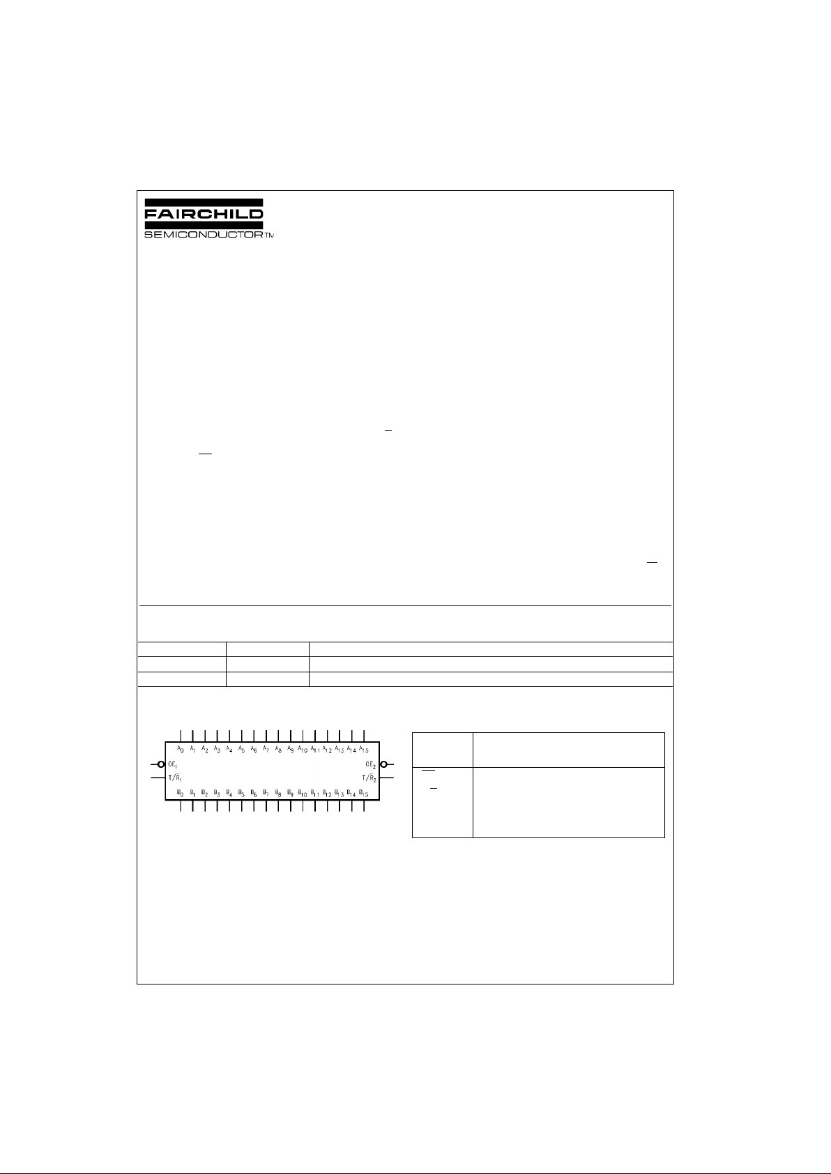
Logic Symbol Pin Descriptions
Order Number Package Number Package Description
74LCXP16245MEA MS48A 48-Lead Small Shrink Outline Package (SSOP), JEDEC MO-118, 0.300” Wide
74LCXP16245MTD MTD48 48-Lead Thin Shrink Small Outline Package (TSSOP), JEDEC MO-153, 6.1mm Wide
Pin Description
Names
OE
n
Output Enable Input
T/R
n
Transmit/Receive Input
A
0–A15
Side A Inputs or 3-STATE Outputs
B
0–B15
Side B Inputs or 3-STATE Outputs
www.fairchildsemi.com 2
74LCXP16245
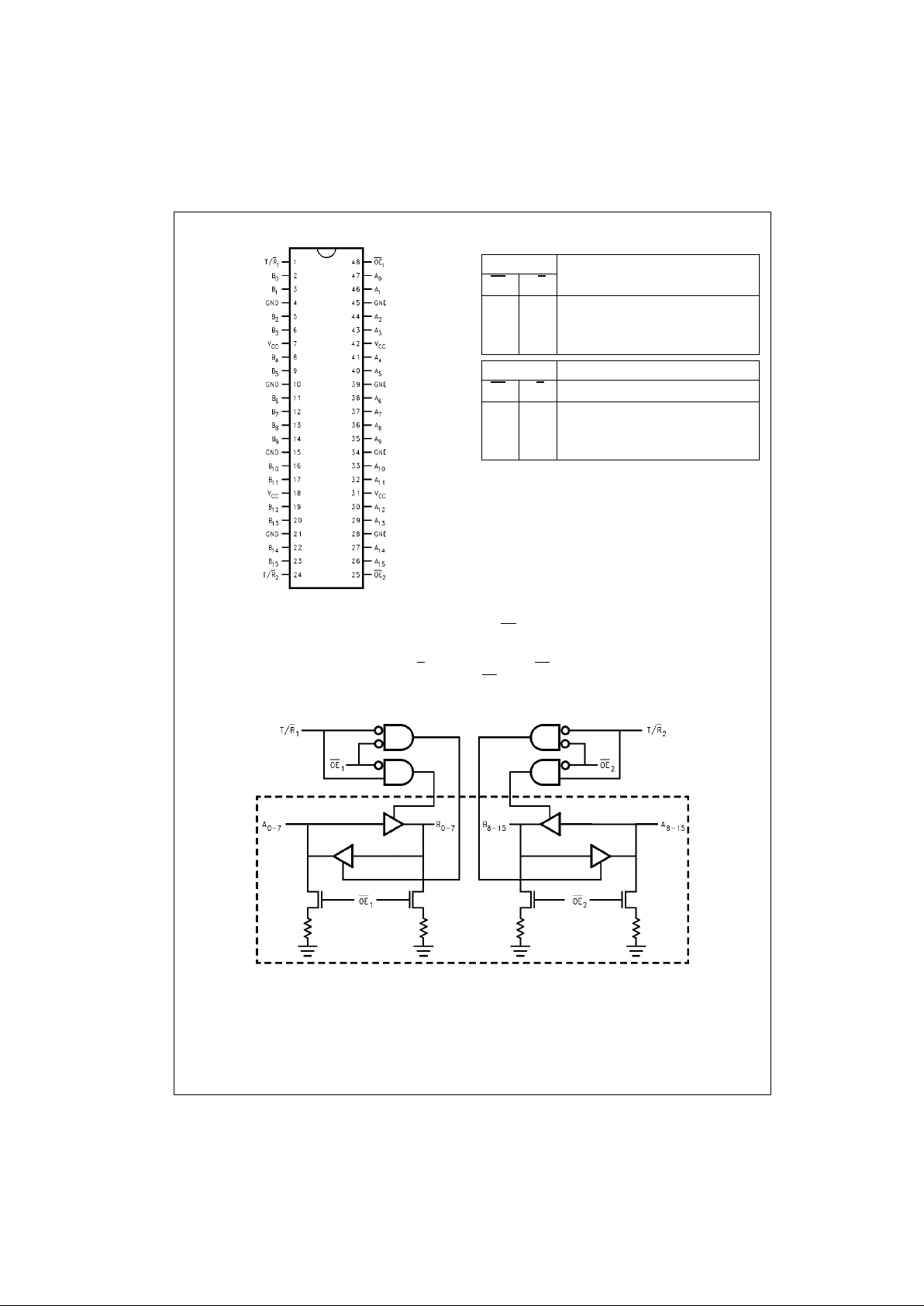
Connection Diagram Tr uth Tables
H = HIGH Voltage Level
L = LOW Voltage Level
X = Immaterial
Z = High Impedance
Note 2: A and B port inputs are still activ e.
Functional Descriptions
The LCXP16245 contains sixteen non-inverting bidirectional buffers with 3-STATE outputs. the device is byte controlled. Each byte has separate control inputs which can be
shorted together for full 16-bit operation . The T/R
inputs
determine the d irection of data flow through the device.
The OE
inputs disable both the A and B po rts by placing
them in a high impedance state. The pulldown resistor
(30KΩ normal) to GND is active only w hen th e output s are
3-STATED (OE
= HIGH). When the o utputs b ecome a ctive
(OE
= LOW) the resistor is removed from the circuit.
Logic Diagram
Inputs Outputs
OE
1
T/R
1
L L Bus B0–B7 Data to Bus A0–A
7
L H Bus A0–A7 Data to Bus B0–B
7
H X HIGH Z State on A0–A7, B0–B7 (Note 2)
Inputs Outputs
OE
2
T/R
2
L L Bus B8–B15 Data to Bus A8–A
15
L H Bus A8–A15 Data to Bus B8–B
15
H X HIGH Z State on A8–A15, B8–B15 (Note 2)
3 www.fairchildsemi.com
74LCXP16245
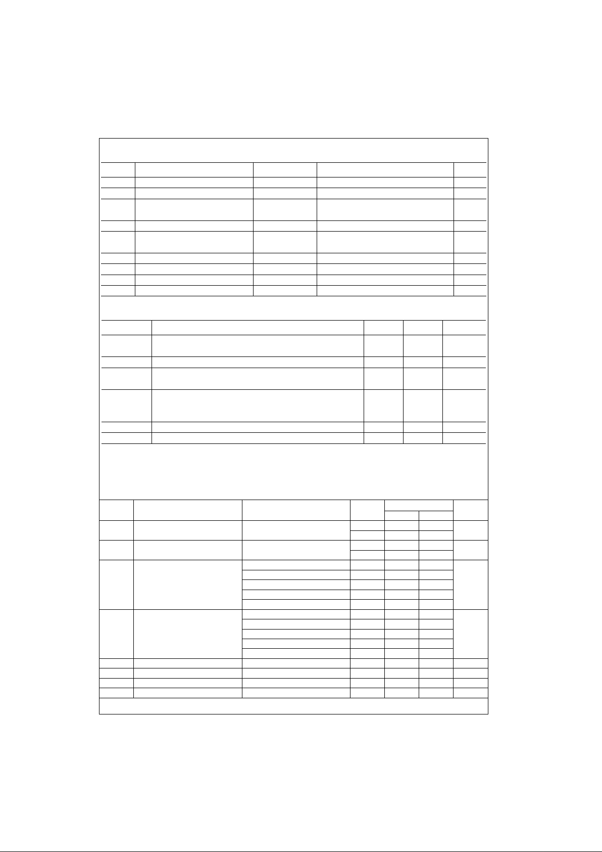
Absolute Maximum Ratings(Note 3)
Recommended Operating Conditions
Note 3: The Absolute Maximum Ratings are those values beyond which the safety of the device cannot be guaranteed. The device should not be operated
at these limits. The parametric values defined in the Electrical Characteristics tables are not guaranteed at the Absolute Maximum Ratings. The “Recommended Operating C onditions” table will define the conditions for act ual device operation.
Note 4: I
O
Absolute Maximum Rating must be observed.
DC Electrical Characteristics
Symbol Parameter Value Conditions Units
V
CC
Supply Voltage −0.5 to +7.0 V
V
I
DC Input Voltage −0.5 to +7.0 V
V
O
DC Output Voltage −0.5 to +7.0 Output in 3-STATE
V
−0.5 to V
CC
+ 0.5 Output in HIGH or LOW State (Note 4)
I
IK
DC Input Diode Current −50 VI < GND mA
I
OK
DC Output Diode Current −50 VO < GND
mA
+50 V
O
> V
CC
I
O
DC Output Source/Sink Current ±50 mA
I
CC
DC Supply Current per Supply Pin ±100 mA
I
GND
DC Ground Current per Ground Pin ±100 mA
T
STG
Storage Temperature −65 to +150 °C
Symbol Parameter Min Max Units
V
CC
Supply Voltage Operating 2.0 3.6
V
Data Retention 1.5 3.6
V
I
Input Voltage 0 5.5 V
V
O
Output Voltage HIGH or LOW State 0 V
CC
V
3-STATE 0 5. 5
I
OH/IOL
Output Current VCC = 3.0V − 3.6V ±24
mA V
CC
= 2.7V − 3.0V ±12
V
CC
= 2.3V − 2.7V ±8
T
A
Free-Air Operating Temperature −40 85 °C
∆t/∆V Input Edge Rate, V
IN
= 0.8V–2.0V, VCC = 3.0V 0 10 ns/V
Symbol Parameter Conditions
V
CC
TA = −40°C to +85°C
Units
(V) Min Max
V
IH
HIGH Level Input Voltage 2.3 − 2.7 1.7
V
2.7 − 3.6 2.0
V
IL
LOW Level Input Voltage 2.3 − 2.7 0.7
V
2.7 − 3.6 0.8
V
OH
HIGH Level Output Voltage IOH = −100 µA 2.3 − 3.6 VCC − 0.2
V
IOH = −8 mA 2.3 1.8
IOH = −12 mA 2.7 2.2
IOH = −18 mA 3.0 2.4
IOH = −24 mA 3.0 2.2
V
OL
LOW Level Output Voltage IOL = 100 µA 2.3 − 3.6 0.2
V
IOL = 8 mA 2.3 0.6
IOL = 12 mA 2.7 0.4
IOL = 16 mA 3.0 0.4
IOL = 24 mA 3.0 0.55
I
I
Input Leakage Current 0 ≤ VI ≤ 5.5V 2.3 − 3.6 ±5.0 µA
I
OZ(L)
3-STATE I/O Leakage VI or VO = 0.0V 2.3 − 3.6 ±5.0 µA
I
OZ(H)
3-STATE I/O Leakage VI or VO = 5.5V 2.3 − 3.6 50 500 µA
I
OFF
Power-Off Leakage Current VI or VO = 5.5V 0 10 µA
 Loading...