

Fairchild Semiconductor 74LCXH32245 Datasheet
April 2002
Revised August 2003
74LCXH32245
Low Voltage 32-Bit Bidirectional Tr ans ceiver
with 5V Tolerant Inputs and Outputs with Bushold
74LCXH32245 Low Voltage 32-Bit Bidirectional Transceiver with 5V Tolerant Inputs and Outputs with Bushold
General Description
The LCXH32245 contains th irty-two non-inverting bidire ctional buffers with 3-STATE outputs and is intended for bus
oriented application s. The device is de signed for low vo ltage (2.5V or 3.3V) V
facing to a 5V signal environment. The device is byte
controlled. Each byte has separate control inputs which
could be shorted toge ther fo r ful l 32-bit op eration . The T /R
inputs determine the direction of data flow through the
device. The OE
placing them in a high impedance state.
The LCXH32245 d ata inputs include bush old, eliminating
the need for external pull-up/do w n resist ors to ho l d unus ed
inputs.
The LCXH32245 is fabricated with an advanced CMOS
technology to achieve high speed operation while maintaining CMOS low power dissipation.
applications with capability of inter-
CC
inputs disable bo th the A and B ports by
Features
■ 5V tolerant inputs and outputs
■ 2.3V to 3.6V V
■ 4.5 ns t
■ Power-off high impedance inputs and outputs
■ Bushold on inputs eliminates the need for external
■ Supports live insertion/withdrawal (Note 1)
■
■ Uses patented noise/EMI reductio n circuitr y
■ Latch-up performance exce eds 500 mA
■ ESD performance:
■ Packaged in plastic Fine-Pitch Ball Grid Array (FBGA)
Note 1: To ensure the high-impedance stat e durin g po wer -up or do wn, OE
should be tied to VCC t hroug h a p ull-up resis tor: the min imu m va lue or t he
resistor is determin ed by the current-sourc ing capability of the driver.
PD
pull-up/down resistors
±24 mA output drive (V
Human body model
Machine model
specifications provided
CC
max (VCC = 3.3V), 20 µA ICC max
> 200V
Ordering Code:
Order Number Package Number Package Description
74LCXH32245G
(Note 2) (Note 3)
Note 2: Ordering Code “G” indicates Trays.
Note 3: Devices also available in Tape and Reel. Specify by appending th e s uffix let t er “X” to the ordering code.
BGA96A 96-Ball Fine-Pitch Ball Grid Array (FBGA), JEDEC MO-205, 5.5mm Wide
Logic Symbol
= 3.0V)
CC
> 2000V
© 2003 Fairchild Semiconductor Corporation DS500727 www.fairchildsemi.com
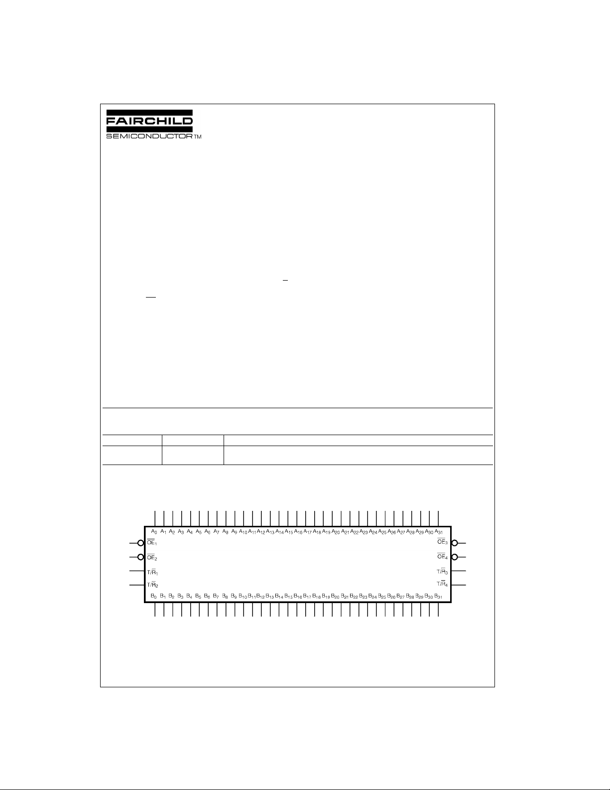
Connection Diagram
74LCXH32245
(Top Thru View)
Pin Descriptions
Pin Names Description
OE
T/R
A
0–A31
B
0–B31
n
n
Output Enable Input (Active LOW)
Transmit/Receive Input
Side A Inputs/3-STATE Outputs
Side B Inputs/3-STATE Outputs
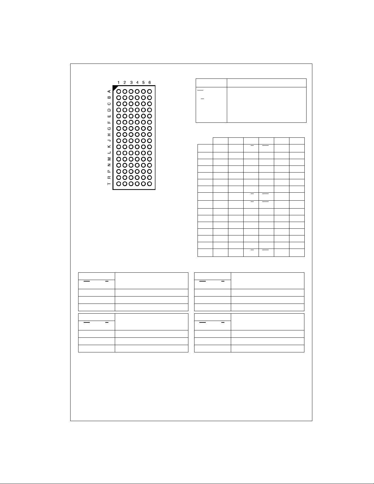
FBGA Pin Assignments
123456
A B
B B
C B
D B
E B
F B11B10V
G B
H B14B15T/R2OE2A
J B
K B19B18GND GND A
L B
M B
N B25B24GND GND A
P B
R B29B28GND GND A
T B
B0T/R1OE1A
1
B2GND GND A2A
3
B4V
5
7
9
13B12
17B16
21B20VCC2VCC2A20A21
23B22
27B26VCC2VCC2A26A27
30B31
CC1VCC1A4
B6GND GND A
B8GND GND A
CC1VCC1A10A11
GND GND A
T/R3OE3A
GND GND A
T/R4OE4A
A
0
A
A
6
A
8
12A13
15A14
16A17
18A19
22A23
24A25
28A29
31A30
1
3
5
7
9
Truth Tables
Inputs
T/R
OE
1
1
L L Bus B0–B7 Data to Bus A0–A
L H Bus A0–A7 Data to Bus B0–B
HXHIGH–Z State on A0–A7,B0–B
Inputs
T/R
OE
2
2
L L Bus B8–B15 Data to Bus A8–A
L H Bus A8–A15 Data to Bus B8–B
H X HIGH–Z State on A8–A15,B8–B
H = HIGH Voltage Level
L = LOW Voltage Level
X = Immaterial
Z = High Impedance
www.fairchildsemi.com 2
Outputs
7
7
7
Outputs
15
15
15
Inputs
OE3T/R
3
Outputs
L L Bus B16–B23 Data to Bus A16–A
L H Bus A16–A23 Data to Bus B16–B
H X HIGH–Z State on A16–A23,B16–B
Inputs
OE4T/R
4
Outputs
L L Bus B24–B31 Data to Bus A24–A
L H Bus B24–A
Data to Bus B24–B
31
H X HIGH–Z State on A24–A31,B24–B
23
23
23
31
31
31
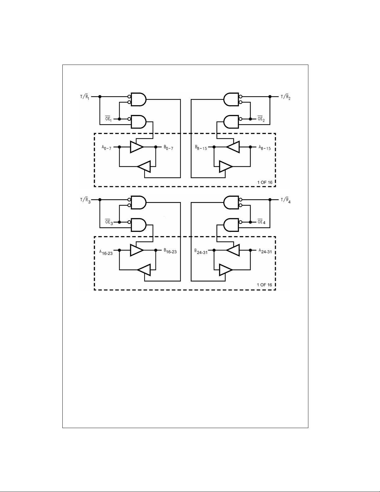
Logic Diagrams
74LCXH32245
Note: Please note that these diagrams are provided only for the unders t anding of logic operatio ns and should not be used to estimate propagation delays.
3 www.fairchildsemi.com
 Loading...