

Fairchild Semiconductor 74LCXH2245 Datasheet
October 2000
Revised September 2001
74LCXH2245
Low Voltage Bidirectional Transceiver with Bushold
and 26
Ω Series Resistors in B Outputs
74LCXH2245 Low Voltage Bidirectional Transceiver with Bushold and 26
General Description
The LCXH2245 contains eight non-inverting bidirectional
buffers with 3-STATE outputs and is in tended for bus oriented applications. The device is designed fo r low voltage
(2.5V and 3.3V) V
mines the direction of data flow through the device. The OE
input disables both the A and B ports by placin g them in a
high impedance state. The 26
output helps reduce output overshoot and undershoot.
The LCXH2245 is fabricated with an advanced CMOS
technology to achieve high speed operation while maintaining CMOS low power dissipation.
The LCXH2245 data inputs include active bushold circuitry,
eliminating the need fo r external pull-up resistors to hold
unused or floating data inputs at a valid logic level.
applications. The T/R input deter-
CC
Ω series resistor in the B Port
Features
■ 5V tolerant control inputs
■ 2.3V–3.6V V
■ Bushold on inputs eliminates the need for external
pull-up/pull-down resistors
■ 7.0 ns t
■ Power down high impedance outputs
■
±12 mA output drive B Port (V
■ Implements patented noise/EMI reduction circuitry
■ Latch-up performance exce eds 500 mA
■ Equivalent 26
■ ESD performance:
Human body model
Machine model
specifications provided
CC
max (V
PD
= 3.3V), 10 µA I
CC
CC
Ω series resistor on B Port outputs
> 2000V
> 200V
CC
= 3.0V)
max
Ordering Code:
Order Number Package Number Package Description
74LCXH2245WM M20B 20-Lead Small Outline Integrated Circuit (SOIC), JEDEC MS-013, 0.300" Wide
74LCXH2245SJ M20D 20-Lead Small Outline Package (SOP), EIAJ TYPE II, 5.3mm Wide
74LCXH2245MSA MSA20 20-Lead Shrink Small Outline Package (SSOP), EIAJ TYPE II, 5.3mm Wide
74LCXH2245MTC MTC20 20-Lead Thin Shrink Small Outline Package (TSSOP), JEDEC MO-153, 4.4mm Wide
Devices also availab l e in Tape and Reel. Specify by appending th e s uffix let t er “X” to the ordering code.
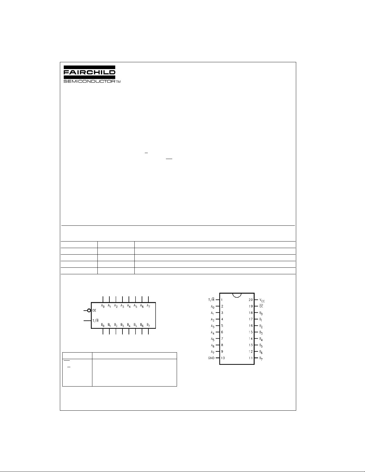
Logic Symbol
Connection Diagram
Ω
Series Resistors in B Outputs
Pin Descriptions
Pin Names Description
OE
T/R
A
0–A7
B
0–B7
GTO is a trademark of Fa irc hild Semiconduct or C orporation.
© 2001 Fairchild Semiconductor Corporation DS500409 www.fairchildsemi.com
Output Enable Input
Transmit/Receive Input
Side A Inputs or 3-STATE Outputs (Bushold)
Side B Inputs or 3-STATE Outputs (Bushold)
Truth Table
74LCXH2245
H = HIGH Voltage Level
L = LOW Voltage Level
X = Immaterial
Z = High Impedance
Logic Diagram
Inputs
OE
T/R
L L Bus B0 – B7 Data to Bus A0 – A
L H Bus A0 – A7 Data to Bus B0 – B
H X HIGH Z State on A0 – A7, B0 – B7
Outputs
7
7
www.fairchildsemi.com 2
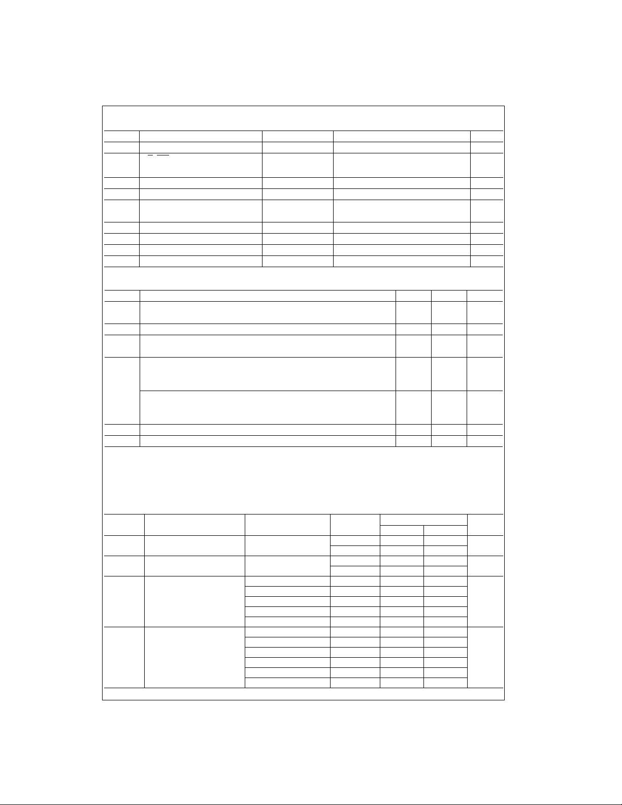
Absolute Maximum Ratings(Note 1)
Symbol Parameter Value Conditions Units
V
V
V
I
I
I
I
I
T
CC
I
O
IK
OK
O
CC
GND
STG
Supply Voltage −0.5 to +7.0 V
T/R, OE, −0.5 to +7.0
I/O Ports
−0.5 to V
+0.5
CC
DC Output Voltage −0.5 to VCC + 0.5 Output in HIGH or LOW State (Note 2) V
DC Input Diode Current −50 VI < GND mA
DC Output Diode Current −50 VO < GND
+50 V
O
> V
CC
DC Output Source/Sink Current ±50 mA
DC Supply Current per Supply Pin ±100 mA
DC Ground Current per Ground Pin ±100 mA
Storage Temperature −65 to +150 °C
Recommended Operating Conditions (Note 3)
Symbol Parameter Min Max Units
V
CC
V
I
V
O
I
OH/IOL
T
A
∆t/∆V Input Edge Rate, V
Note 1: The Absolute Maximum Ratings are those values beyond which the safety of the device cannot be guaranteed. The device should not be operated
at these limits. The parametric values defined in the Electrical Characteristics tables are not guaranteed at the Absolute Maximum Ratings. The “Recom-
mended Operating Conditions” table will define th e c onditions for actual dev ic e operation.
Note 2: I
Note 3: Floati ng or unused control inputs must be HIGH or LOW.
Supply Voltage Operating 2.0 3.6
Data Retention 1.5 3.6
Input Voltage 0VCCV
Output Voltage HIGH or LOW State 0 V
CC
3-STATE 0 5.5
Output Current in IOH/IOL - A Outputs VCC = 3.0V − 3.6V ±24
= 2.7V - 3.0V ±12
CC
= 2.3V - 2.7V ± 8
V
Output Current in I
- B Outputs VCC = 3.0V − 3.6V ±12
OH/IOL
CC
= 2.7V - 3.0V ± 8
CC
= 2.3V - 2.7V ± 4
V
CC
Free-Air Operating T emperature −40 85 °C
= 0.8V − 2.0V, VCC = 3.0V 0 10 ns/V
IN
Absolute Maximum Rating must be observed.
O
mAV
mAV
74LCXH2245
V
mA
V
V
DC Electrical Characteristics
Symbol Parameter Conditions
V
IH
V
IL
V
OH
V
OH
HIGH Level Input Voltage 2.3 − 2.7 1.7
LOW Level Input Voltage 2.3 − 2.7 0.7
HIGH Level Output Voltage IOH = −100 µA 2.3 - 3.6 VCC − 0.2
A Outputs IOH = −8 mA 2.3 1.8
IOH = −12 mA 2.7 2.2
IOH = −16 mA 3.0 2.4
IOH = −24 mA 3.0 2.2
HIGH Level Output Voltage IOH = −100 µA 2.3 - 3.6 VCC − 0.2
B Outputs IOH = −4 mA 2.3 1.8
IOH = −4 mA 2.7 2.2
IOH = −6 mA 3.0 2.4
IOH = −8 mA 2.7 2.0
IOH = −12 mA 3.0 2.0
V
CC
(V) Min Max
2.7 − 3.6 2.0
2.7 - 3.6 0.8
TA = −40°C to +85°C
Units
V
V
V
V
3 www.fairchildsemi.com
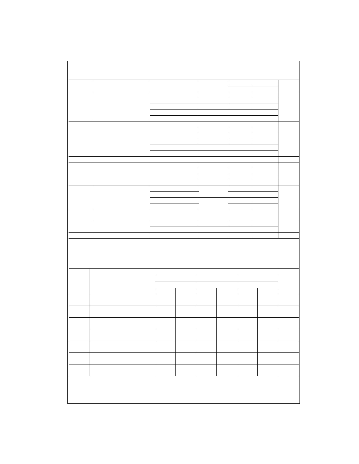
DC Electrical Characteristics (Continued)
Symbol Parameter Conditions
V
OL
74LCXH2245
LOW Level Output Voltage IOL = 100 µA2.3 − 3.6 0.2
A Outputs I
= 8 mA 2.3 0.6
OL
I
= 12 mA 2.7 0.4
OL
IOL = 16 mA 3.0 0.4
= 24 mA 3.0 0.55
I
V
OL
LOW Level Output Voltage IOL = 100 µA2.3 − 3.6 0.2
OL
B Outputs IOL = 4 mA 2.3 0.6
= 4 mA 2.7 0.4
I
OL
I
= 6 mA 3.0 0.55
OL
IOL = 8 mA 2.7 0.6
= 12 mA 3.0 0.8
I
I
I
I
I(HOLD)
Input Leakage Current VI = VCC or GND 2.3 − 3.6 ±5.0 µA
Bushold Input Minimum VIN = 0.7V
OL
Drive Hold Current VIN = 1.7V −45
VIN = 0.8V
VIN = 2.0V −75
I
I(OD)
Bushold Input Over-Drive (Note 5)
Current to Change State (Note 6) −300
(Note 5)
(Note 6) −450
I
OZ
I
CC
3-STATE I/O Leakage VO = VCC or GND
VI = VIH or V
IL
Quiescent Supply Current VI = VCC or GND 2.3 − 3.6 10
3.6V ≤ VI, VO ≤ 5.5V (Note 4) 2.3 − 3.6 ±10
∆I
CC
Note 4: Outputs disabled or 3- STATE only.
Note 5: An external driver must source at least the specified current to switch from LOW-to-HIGH.
Note 6: An external driver must s ink at least the specified current to switch from HI GH-to-LOW.
Increase in ICC per Input VIH = VCC −0.6V 2.3 - 3.6 500 µA
V
CC
(V) Min Max
2.3
3.0
2.7
3.6
TA = −40°C to +85°C
45
75
300
450
Units
2.3 − 3.6 ±5.0 µA
V
V
µA
µA
µA
AC Electrical Characteristics
TA = −40°C to +85°C, RL = 500Ω
V
= 3.3V ± 0.3V VCC = 2.7V VCC = 2.5V ± 0.2V
Symbol Parameter
t
PHL
t
PLH
t
PHL
t
PLH
t
PZL
t
PZH
t
PZL
t
PZH
t
PLZ
t
PHZ
t
PLZ
t
PHZ
t
OSHL
t
OSLH
Note 7: Skew is defined as the absolute value of the difference between the actual propagation delay for any two separate outputs of the same device. The
specification applies to any outputs sw it c hing in the same direction, either HIGH-to-LOW (t
Propagation Delay
A to B
Propagation Delay
B to A
Output Enable Time
A to B
Output Enable Time
B to A
Output Disable Time
A to B
Output Disable Time
B to A
Output to Output Skew
(Note 7)
www.fairchildsemi.com 4
CC
= 50 pF CL = 50 pF CL = 30 pF
C
L
Min Max Min Max Min Max
1.58.01.59.01.59.6ns
1.57.01.58.01.58.4ns
1.5 9.5 1.5 10.5 1.5 11.0 ns
1.58.51.59.51.510.5ns
1.57.51.58.51.59.0ns
1.57.51.58.51.59.0ns
1.0 ns
) or LOW-to-HIGH (t
OSHL
OSLH
).
Units
 Loading...