

Fairchild Semiconductor 74LCXH16374 Datasheet
February 2001
Revised June 2002
74LCXH16374
Low Voltage 16-Bit D-Type Flip-Flop with Bushold
74LCXH16374 Low Voltage 16-Bit D-Type Flip-Flop with Bushold
General Description
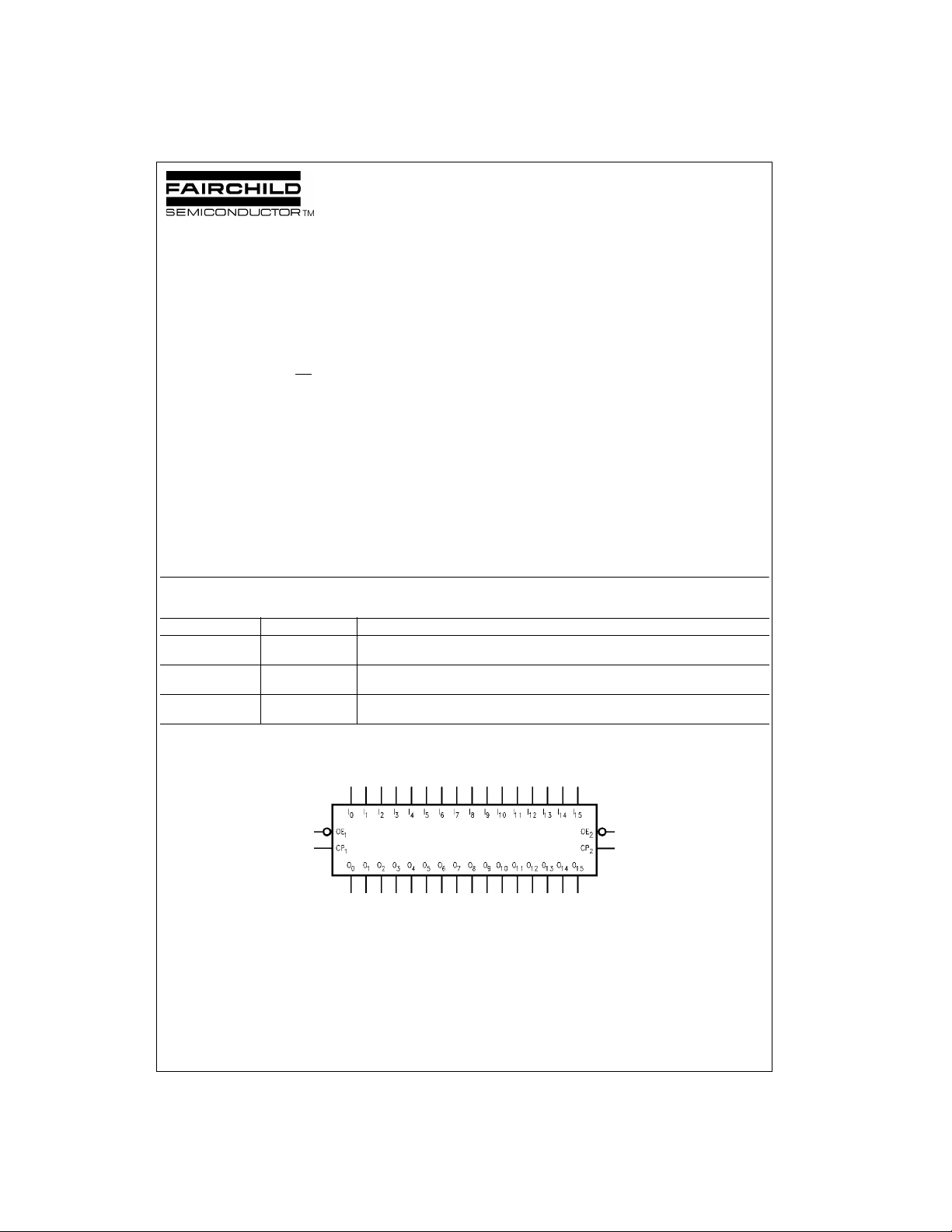
The LCXH16374 contains sixteen non-inverting D-type flipflops with 3-STATE outputs and is intended for bus oriented
applications. The device is byte controlled. A buffered clock
(CP) and Output E nable (OE
and can be shorted together for full 16-bit operation.
The LCXH16374 is designed for low voltage (2.5V or 3.3V)
V
applications.
CC
The LCXH16374 is fabricated with an advanced CMOS
technology to achieve high speed operation while maintaining CMOS low power dissipation.
The LCXH16374 data inputs include active bushold circuitry, eliminating the need for external pull-up resistors to
hold unused or floating data inputs at a valid logic level.
) are common to each byte
Features
■ 5V tolerant control inputs and outputs
■ 2.3V–3.6V V
■ 6.2 ns t
■ Bushold on inputs eliminating the need for external
pull-up/pull-down resistors
■ Power down high impedance outputs
■
±24 mA output drive (V
■ Implements patented noise/EMI reduction circuitry
■ Latch-up performance exce eds 500 mA
■ ESD performance:
Human body model
Machine model
■ Also packaged in plastic Fine-Pitch Ball Grid Array
(FBGA)
specifications provided
CC
max (VCC = 3.3V), 20 µA ICC max
PD
> 200V
Ordering Code:
Order Number Package Number Package Description
74LCXH16374G
(Note 1)(Note 3)
74LCXH16374MEA
(Note 2)
74LCXH16374MTD
(Note 2)
Note 1: Ordering code “G” indicates Trays.
Note 2: Devices also available in Tape and Reel. Specify by appending th e s uffix let t er “X” to the ordering code.
BGA54A 54-Ball Fine-Pitch Ball Grid Array (FBGA), JEDEC MO-205, 5.5mm Wide
MS48A 48-Lead Small Shrink Outline Package (SSOP), JEDEC MO-118, 0.300" Wide
MTD48 48 - Le ad T hi n Shr i n k S m all Ou t li n e P ac ka ge ( TS S OP ), J E DE C MO - 15 3 , 6. 1m m W i de
Logic Symbol
= 3.0V)
CC
> 2000V
GTO is a trademark of Fa irc hild Semiconduct or C orporation.
© 2002 Fairchild Semiconductor Corporation DS500441 www.fairchildsemi.com
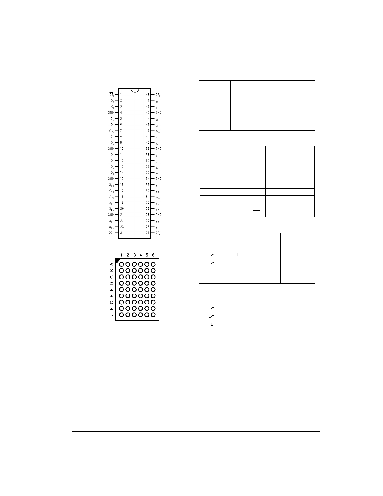
Connection Diagrams
Pin Descriptions
Pin Assignment for SSOP and TSSOP
74LCXH16374
Pin Assignment for FBGA
Pin Names Description
OE
CP
I
0–I15
O
0–O15
n
n
Output Enable Input (Active LOW)
Clock Pulse Input
Bushold Inputs
Outputs
NC No Connect
FBGA Pin Assignments
123456
A O
B O
C O
D O
E O
F O
G O
H O
J O
NC OE1CP1NC I
0
O1NC NC I
2
O3V
4
6
8
10
12O11VCCVCCI11
14O13
15
CCVCCI3
O5GND GND I
O7GND GND I
O9GND GND I
NC NC I
NC OE2CP2NC I
1
5
7
9
13I14
Truth Tables
Inputs Outputs
CP
1
LL X O
XH X Z
OE
1
I0–I
7
O0–O
LH H
LL L
0
I
2
I
4
I
6
I
8
I
10
I
12
15
7
0
(Top Thru View)
www.fairchildsemi.com 2
Inputs Outputs
CP
2
OE
2
I8–I
15
O8–O
LH H
LL L
LL X O
XH X Z
H = HIGH Voltage Level
L = LOW Voltage Level
X = Immaterial
Z = High Impedance
= Previous O0 before HIGH-to-LOW of CP
O
0
15
0
Functional Description
The LCXH16374 consists of sixteen edge-triggered
flip-flops with individual D-type inputs and 3-STATE true
outputs. The device i s byte contr olled wit h each byte func tioning identically, but independent of the other. The control
pins can be shorted to gether to obtain f ull 1 6-b it o per ati o n.
Each byte h a s a bu ffered cloc k a nd bu ffered Outp ut En ab le
common to all flip-flops within that byte. The description
which follows applies to each byte. Each flip-flop will store
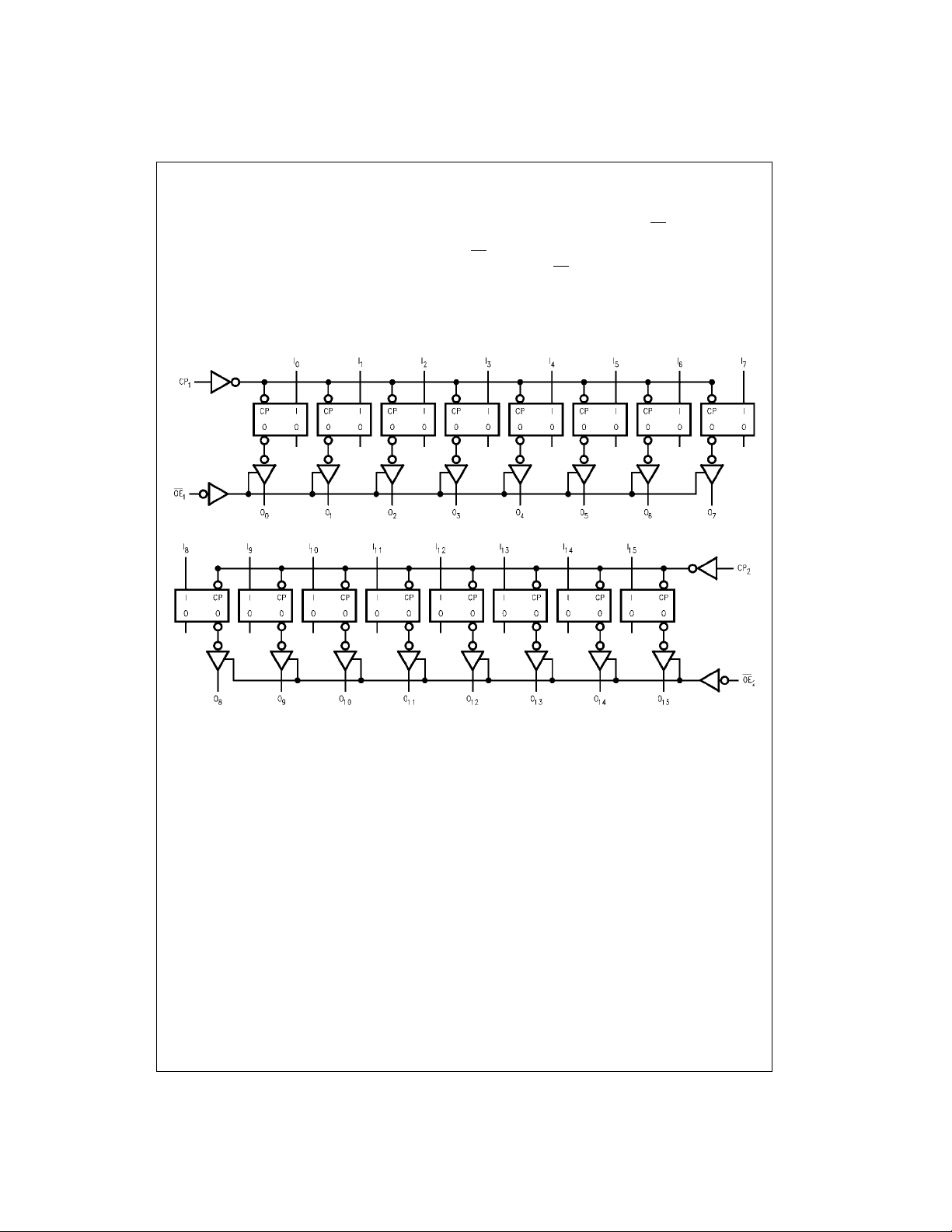
Logic Diagrams
Byte 1 (0:7)
Byte 2 (8:15)
the state of their individual D inputs that meet the setup and
hold time requirements on t he LOW-to-HIGH Clock (CP
transition. With the Output Enable (OE
tents of the flip-flops ar e available at the outputs. When
OE
is HIGH, the outputs go to the high impedan ce state.
n
Operation of the OE
flip-flops.
input does not affect the stat e of the
n
) LOW, the con-
n
74LCXH16374
)
n
Please note that this diagram is provided only for the understanding of logic operations and should not be used to estimate propagation delays.
3 www.fairchildsemi.com
 Loading...