

Fairchild Semiconductor 74LCXH16373 Datasheet
February 2001
Revised August 2001
74LCXH16373
Low Voltage 16-Bit Transparent Latch with Bushold
74LCXH16373 Low Voltage 16-Bit Transparent Latch with Bushold
General Description
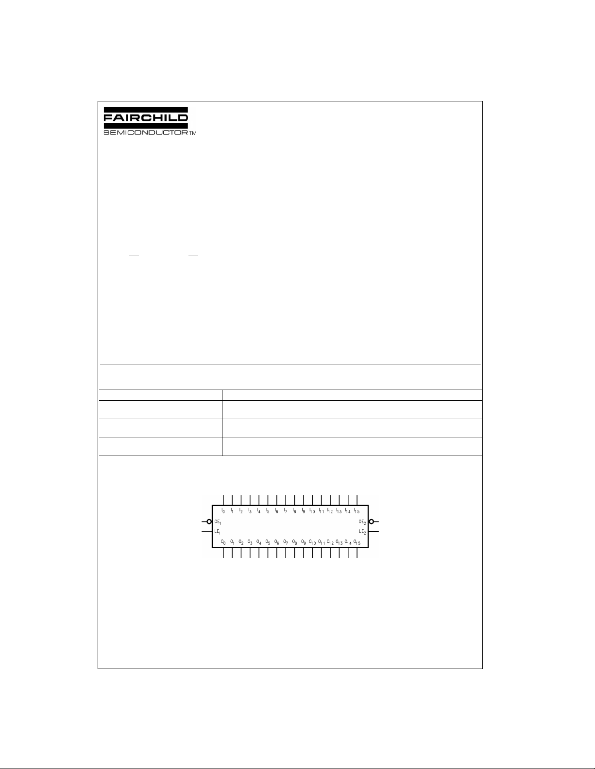
The LCXH16373 contains sixteen non-inverting latches
with 3-STATE outputs and is intended for bus oriented
applications. The device is byte controlled. The flip-flops
appear transparent to the data when the Latch Enable (LE)
is HIGH. When LE is LOW, the data that meets the setup
time is latched. Data appears o n the bus when th e Output
Enable (OE
a high impedance state.
The LCXH16373 is designed for low voltage (2.5V or 3.3V)
V
CC
environment.
The LCXH16373 is fabricated with an advanced CMOS
technology to achieve high speed operation while maintaining CMOS low power dissipation.
The LCXH16373 data inputs include active bushold circuitry, eliminating the need for external pull-up resistors to
hold unused or floating data input at a valid logic level.
) is LOW. When OE is HIGH, the outputs are in
applications with capability of interfacing to a 5V signal
Features
■ 5V tolerant control inputs and outputs
■ 2.3V–3.6V V
■ 5.4 ns t
■ Bushold on inputs eliminates the need for external
pull-up/pull-down resistors
■ Power down high impedance outputs
■
±24 mA output drive (V
■ Implements patented noise/EMI reduction circuitry
■ Latch-up performance exce eds 500 mA
■ ESD performance:
Human body model
Machine model
■ Also available in plastic Fine-Pitch Ball Grid Array
(FBGA) (Preliminary)
specifications provided
CC
max (VCC = 3.3V), 20 µA ICC max
PD
> 200V
Ordering Code:
Order Number Package Number Package Description
74LCXH16373GX
(Note 1)
74LCXH16373MEA
(Note 2)
74LCXH16373MTD
(Note 2)
Note 1: BGA package available in Tape and Reel only.
Note 2: Devices also available in Tape and Reel. Specify by appending th e s uffix let t er “X” to the ordering code.
BGA54A
(Preliminary)
MS48A 48-Lead Small Shrink Outline Package (SSOP), JEDEC MO-118, 0.300" Wide
MTD48 48-Lead Thin Shrink Small Outline Package (TSSOP), JEDEC MO-153, 6.1mm Wide
54-Ball Fine-Pitch Ball Grid Array (FBGA), JEDEC MO-205, 5.5mm Wide
[TAPE and REEL]
= 3.0V)
CC
> 2000V
Logic Symbol
© 2001 Fairchild Semiconductor Corporation DS500440 www.fairchildsemi.com
Connection Diagrams
Pin Descriptions
Pin Assignment for SSOP and TSSOP
74LCXH16373
Pin Assignment for FBGA
(Top Thru View)
Pin Names Description
OE
LE
I
0–I15
O
0–O15
n
n
Output Enable Input (Active LOW)
Latch Enable Input
Bushold Inputs
Outputs
NC No Connect
FBGA Pin Assignments
123456
A O
B O
C O
D O
E O
F O
G O
H O
J O
NC OE1LE1NC I
0
O1NC NC I
2
O3V
4
6
8
10
12O11VCCVCCI11
14O13
15
CCVCCI3
O5GND GND I
O7GND GND I
O9GND GND I
NC NC I
NC OE2LE2NC I
1
5
7
9
13I14
Truth Tables
Inputs Outputs
LE
1
XH X Z
HL L L
HL H H
LL X O
LE
2
XH X Z
HL L L
HL H H
LL X O
H = HIGH Voltage Level
L = LOW Voltage Level
X = Immaterial
Z = High Impedance
= Previous O0 before HIGH-to-LOW transition of Lat ch Enable
O
0
OE
1
I0–I
7
O0–O
Inputs Outputs
OE
2
I8–I
15
O8–O
0
I
2
I
4
I
6
I
8
I
10
I
12
15
7
0
15
0
www.fairchildsemi.com 2
Functional Description
The LCXH16373 contains sixteen D-type latches with
3-STATE standard outputs. The device is byte controlled
with each byte functioning iden tically, but independent of
the other. Cont r ol pins can be s h or t ed t o ge t he r to o b t ain f u l l
16-bit operation. The foll owing description ap plies to each
byte. When the Latch Enable (LE
enters the latches. In this condit ion the latches are
the I
n
transparent, i.e. a latch outpu t will change state each time
) input is HIGH, data on
n
Logic Diagrams
its I input changes. When LE
information that was present on the I inputs a setup time
preceding the HIGH-to-LOW transition of LE
3-STATE standard outputs are controlled by the Output
Enable (OE
puts are in the 2-state mode. When OE
dard outputs are in the high impedance mode but this does
not interfere with entering new data into the latches.
) input. When OEn is LOW, the standard out-
n
is LOW, the latches store
n
. The
n
is HIGH, the stan-
n
74LCXH16373
Please note that this diagram is provided only for the understanding of logic operations and should not be used to estimate propagation delays.
3 www.fairchildsemi.com
Absolute Maximum Ratings(Note 3)
Symbol Parameter Value Conditions Units
V
CC
V
I
74LCXH16373
V
O
I
IK
I
OK
I
O
I
CC
I
GND
T
STG
Supply Voltage −0.5 to +7.0 V
DC Input Voltage I0 - I
OE
n
, LE
−0.5 to V
15
−0.5V to 7.0V
n
CC
+ 0.5
DC Output Voltage −0.5 to +7.0 Output in 3-STA TE
−0.5 to V
+ 0.5 Output in HIGH or LOW State (Note 4)
CC
DC Input Diode Current −50 VI < GND mA
DC Output Diode Current −50 VO < GND
+50 V
> V
O
CC
DC Output Source/Sink Current ±50 mA
DC Supply Current per Supply Pin ±100 mA
DC Ground Current per Ground Pin ±100 mA
Storage Temperature −65 to +150 °C
Recommended Operating Conditions (Note 5)
Symbol Parameter Min Max Units
V
CC
V
I
V
O
I
OH/IOL
T
A
∆t/∆V Input Edge Rate, V
Note 3: The Absolute Maximum Ratings are those values beyond which the safety of the device cannot be guaranteed. The device should not be operated
at these limits. The parametric values defined in the Electrical Characteristics tables are not guaranteed at the Absolute Maximum Ratings. The “Recom-
mended Operat ing Conditions” table w ill define the condition s fo r ac t ual device operation.
Note 4: I
Note 5: Floating or unused control inputs must be HIGH or LOW.
Supply Voltage Operating 2.0 3.6
Data Retention 1.5 3.6
Input Voltage 0 V
Output Voltage HIGH or LOW State 0 V
CC
CC
3-STATE 0 5.5
Output Current VCC = 3.0V − 3.6V ±24
= 2.7V − 3.0V ±12
CC
= 2.3V − 2.7V ±8
V
CC
Free-Air Operating Temperature −40 85 °C
= 0.8V–2.0V, VCC = 3.0V 0 10 ns/V
IN
Absolute Maximum Rating must be observed.
O
V
V
mA
V
V
V
mAV
DC Electrical Characteristics
Symbol Parameter Conditions
V
IH
V
IL
V
OH
V
OL
I
I
www.fairchildsemi.com 4
HIGH Level Input Voltage 2.3 − 2.7 1.7
LOW Level Input Voltage 2.3 − 2.7 0.7
HIGH Level Output Voltage IOH = −100 µA2.3 − 3.6 VCC − 0.2
IOH = 8 mA 2.3 1.8
IOH = −12 mA 2.7 2.2
IOH = −18 mA 3.0 2.4
IOH = −24 mA 3.0 2.2
LOW Level Output Voltage IOL = 100 µA2.3 − 3.6 0.2
IOL = 8 mA 2.3 0.6
IOL = 12 mA 2.7 0.4
IOL = 16 mA 3.0 0.4
IOL = 24 mA 3.0 0.55
Input Leakage Current VI = VCC or GND 2.3 − 3.6 ±5.0 µA
V
2.7 − 3.6 2.0
2.7 − 3.6 0.8
TA = −40°C to +85°C
CC
(V) Min Max
Units
V
V
V
V
 Loading...