

Fairchild Semiconductor 74LCXH162244MTX, 74LCXH162244MTD, 74LCXH162244MEX, 74LCXH162244MEA Datasheet
September 2000
Revised September 2000
74LCXH162244
Low Voltage 16-Bit Buffer/Line Driver with Bushold
and 26
Ω Series Resistors in Outputs
74LCXH162244 Low Voltage 16-Bit Buffer/Line Driver with Bushold and 26
General Description
The LCXH162244 contains sixteen non-inverting buffers
with 3-STA TE outputs designed to be employed as a memory and address driver, clock driver, or bus oriented transmitter/receiver. The device is nibble controlled. Each nibble
has separate 3-STATE control inputs which can be shorted
together for full 16-bit operation.
The LCXH162244 da ta inputs include active bushol d circuitry, eliminating the need for external pull-up resistors to
hold unused or floating data inputs at a valid logic level.
In addition, the outputs incl ude equivalent 26
series resistors to reduce overshoot and undershoot and
are designed to sink/source up to 12 mA at V
The LCXH162244 is designed for low voltage (2.5V or
3.3V) V
signal environment.
The LCXH162244 is fa bricated with an advanced CMOS
technology to achieve high speed operation while maintaining CMOS low power dissipation.
applications with capability of interfacing to a 5V
CC
Ω (nominal)
= 3.0V.
CC
Features
■ 5V tolerant control inputs and outputs
■ 2.3V–3.6V V
■ Outputs include equiv alent series resistance of 26
make external termination resistors unnecessary and
reduce overshoot and undershoot
■ Bushold on data inputs eliminates the need for external
pull-up/pull-down resistors
■ 5.3 ns t
■ Power down high impedance inputs and outputs
■
±12 mA output drive (V
■ Implements patented noise/EMI reduction circuitry
■ Latch-up performance exce eds 500 mA
■ ESD performance:
Human body model
Machine model
specifications provided
CC
max (VCC = 3.0V), 20 µA ICC max
PD
= 3.0V)
CC
> 2000V
> 200V
Ω to
Ordering Code:
Order Number Package Number Package Description
74LCXH162244MEA MS48A 48-Lead Small Shrink Outline Package (SSOP), JEDEC MO-118, 0.300 Wide
74LCXH162244MTD MTD48 48-Lead Thin Shrink Small Outline Package (TSSOP), JEDEC MO-153, 6.1mm Wide
Devices also availab l e in Tape and Reel. Specify by appending th e s uffix let t er “X” to the ordering code.
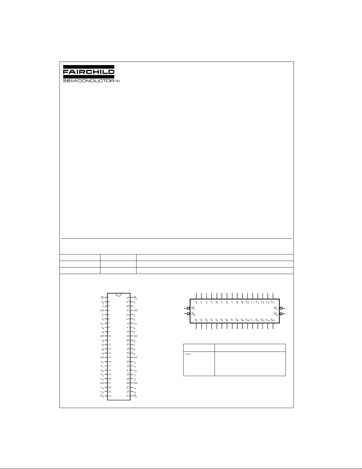
Connection Diagram Logic Symbol
Ω
Series Resistors in Outputs
Pin Descriptions
Pin Names Description
OE
n
I
0–I15
O
0–O15
© 2000 Fairchild Semiconductor Corporation DS500249 www.fairchildsemi.com
Output Enable Input (Active LOW)
Bushold Inputs
Outputs
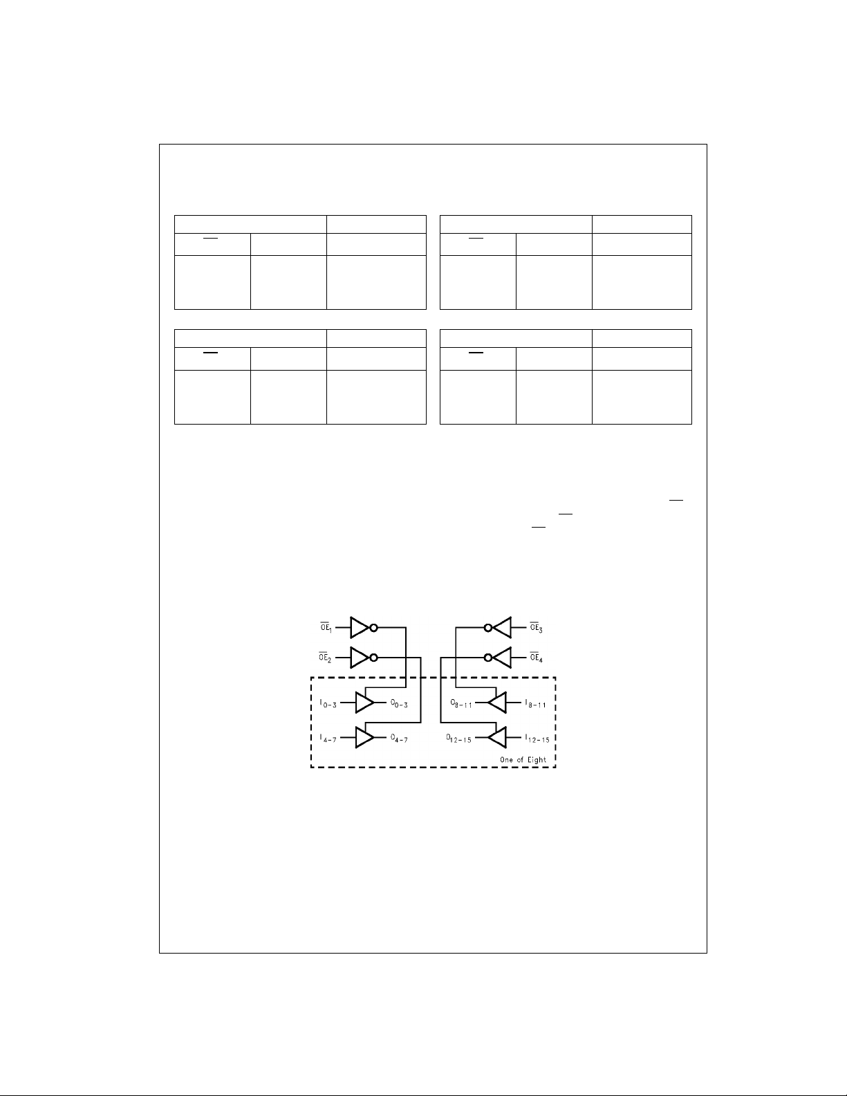
Truth Tables
Inputs Outputs Inputs Outputs
OE
74LCXH162244
1
I0–I
3
O0–O
LL L LL L
LH H LH H
HX Z HX Z
Inputs Outputs Inputs Outputs
OE
2
I4–I
7
O4–O
LL L LL L
LH H LH H
HX Z HX Z
H = HIGH Voltage Level
L = LOW Voltage Level
Functional Description
The LCXH162244 contains sixteen non-inverting buffers
with 3-STATE standard outputs. The LCXH162244 data
inputs include active bu shold circuit ry eliminatin g the need
for pull-up resistors to hold unused or floating data inputs at
a valid logic level. T he devise is also designed with 26
series resistors in the outputs. This design reduces line
noise in applications such as memory address drivers,
clock drivers and bu s transceiver/tran smitters. The de vice
is nibble (4 bits) controlled with each nibble functioning
3
7
OE
3
OE
4
X = Immaterial
Z = High Impedance
I8–I
I12–I
11
15
O8–O
O12–O
11
15
identically, but independent of the other. The control pins
can be shorted toge ther to ob tain full 1 6-bit op eration . The
3-STATE outputs are controlled by an Output Enable (OE
input for each nibble. When OE
Ω
2-state mode. Wh en OE
is LOW, the outputs are in
n
is HIGH, the outputs are in the
n
)
n
high impedance mode, but this does not interfere with
entering new data into the inputs.
Logic Diagram
www.fairchildsemi.com 2
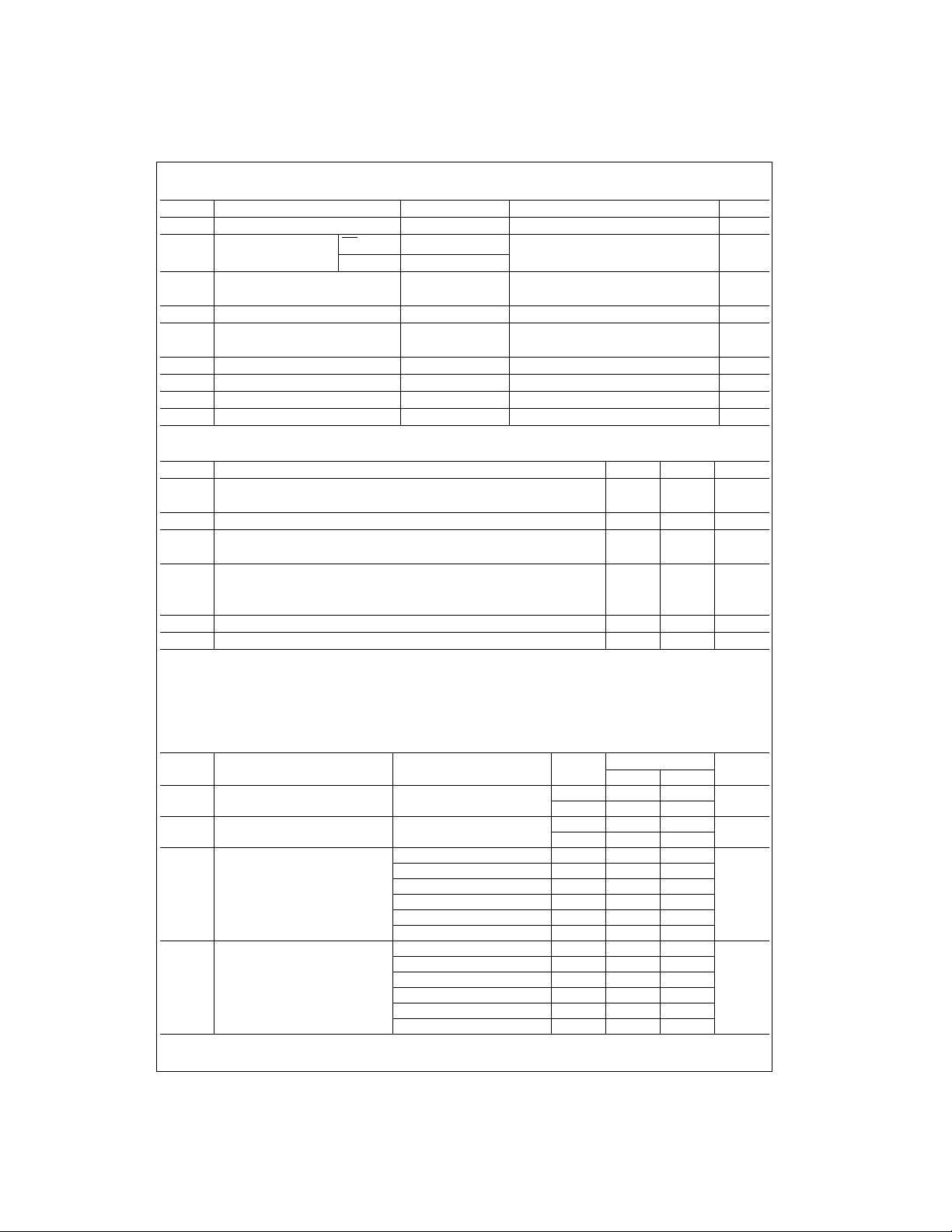
Absolute Maximum Ratings(Note 1)
Symbol Parameter Value Conditions Units
V
V
V
I
IK
I
OK
I
O
I
CC
I
GND
T
CC
I
O
STG
Supply Voltage −0.5 to +7.0 V
DC Input Voltage OE −0.5 to +7.0
- I
I
0
15
−0.5 to V
CC
+ 0.5
DC Output Voltage −0.5 to +7.0 Output in 3-STATE
−0.5 to V
+ 0.5 Output in HIGH or LOW State (Note 2)
CC
DC Input Diode Current −50 VI < GND mA
DC Output Diode Current −50 VO < GND
+50 V
O
> V
CC
mA
DC Output Source/Sink Current ±50 mA
DC Supply Current per Supply Pin ±100 mA
DC Ground Current per Ground Pin ±100 mA
Storage Temperature −65 to +150 °C
Recommended Operating Conditions (Note 3)
Symbol Parameter Min Max Units
V
CC
V
I
V
O
I
OH/IOL
T
A
∆t/∆V Input Edge Rate, V
Note 1: The Absolute Maximum Ratings are those values beyond which the safety of the device cannot be guaranteed. The device should not be operated
at these limits. The parametric values defined in the Electrical Characteristics tables are not guaranteed at the Absolute Maximum Ratings. The “Recom-
mended Operating Conditions” table will define the conditions fo r ac t ual device operation.
Note 2: I
Note 3: Unused control inputs m us t be held HIGH or LOW. They ma y n ot flo at .
Supply Voltage Operating 2.0 3.6
Data Retention 1.5 3.6
Input Voltage 0VCCV
Output Voltage HIGH or LOW State 0 V
CC
3-STATE 0 5.5
Output Current VCC = 3.0V − 3.6V ±12
= 2.7V − 3.0V ±8
CC
V
= 2.3V − 2.7V ±4
CC
Free-Air Operating T emperature −40 85 °C
= 0.8V–2.0V, VCC = 3.0V 0 10 ns/V
IN
Absolute Maximum Rating must be observed.
O
mAV
74LCXH162244
V
V
V
V
DC Electrical Characteristics
Symbol Parameter Conditions
V
IH
V
IL
V
OH
V
OL
HIGH Level Input Voltage 2.3 − 2.7 1.7
LOW Level Input Voltage 2.3 − 2.7 0.7
HIGH Level Output Voltage IOH = −100 µA2.3 − 3.6 VCC − 0.2
IOH = −4 mA 2.3 1.8
IOH = −4 mA 2.7 2.2
IOH = −6 mA 3.0 2.4
IOH = −8 mA 2.7 2.0
IOH = −12 mA 3.0 2.0
LOW Level Output Voltage IOL = 100 µA2.3 − 3.6 0.2
IOL = 4 mA 2.3 0.6
IOL = 4 mA 2.7 0.4
IOL = 6 mA 3.0 0.55
IOL = 8 mA 2.7 0.6
IOL = 12 mA 3.0 0.8
3 www.fairchildsemi.com
V
TA = −40°C to +85°C
CC
(V) Min Max
2.7 − 3.6 2.0
2.7 − 3.6 0.8
Units
V
V
V
V
 Loading...