

Fairchild Semiconductor 74LCX841WMX, 74LCX841WM, 74LCX841MTCX, 74LCX841MTC, 74LCX841MSAX Datasheet
...
October 1995
Revised April 1999
74LCX841 Low Voltage 10-Bit Transparent Latch with 5V Tolerant Inputs and Outputs
© 1999 Fairchild Semiconductor Corporation DS012575.prf www.fairchildsemi.com
74LCX841
Low Voltage 10-Bit Transparent Latch with 5V Tolerant
Inputs and Outputs
General Description
The LCX841 consist s of ten latches w ith 3-STATE outputs
for bus organized system applications. The device is
designed for low volta ge (2.5V or 3.3V) V
CC
applications
with capability of interfacing to a 5V signal environment.
The LCX841 is fabrica ted with an advanced CMOS tech-
nology to achieve high spee d operation while mai ntaining
CMOS low power dissipation.
Features
■ 5V tolerant inputs and outputs
■ 2.3V − 3.6V V
CC
specifications provided
■ 8.0 ns t
PD
max (VCC = 3.3V), 10 µA ICC max
■ Power-down high impedance inputs and outputs
■ Supports live insertion/withdrawal (Note 1)
■ ±24 mA output drive (V
CC
= 3.0V)
■ Implements patented noise/EMI reduction circuitry
■ Latch-up performance exceeds 500 mA
■ ESD performance:
Human Body Model > 200 0V
Machine Model > 200V
Note 1: To ensure the high-impedan c e state during power up or down, OE
should be tied to VCC through a pull-up res istor: the m inimu m value or t he
resistor is determin ed by the current-sourcing capability of the dr iv er.
Ordering Code:
Devices also availab le in Tape and Reel. Specify by appending th e s uffix let t er “X” to the ordering cod e.
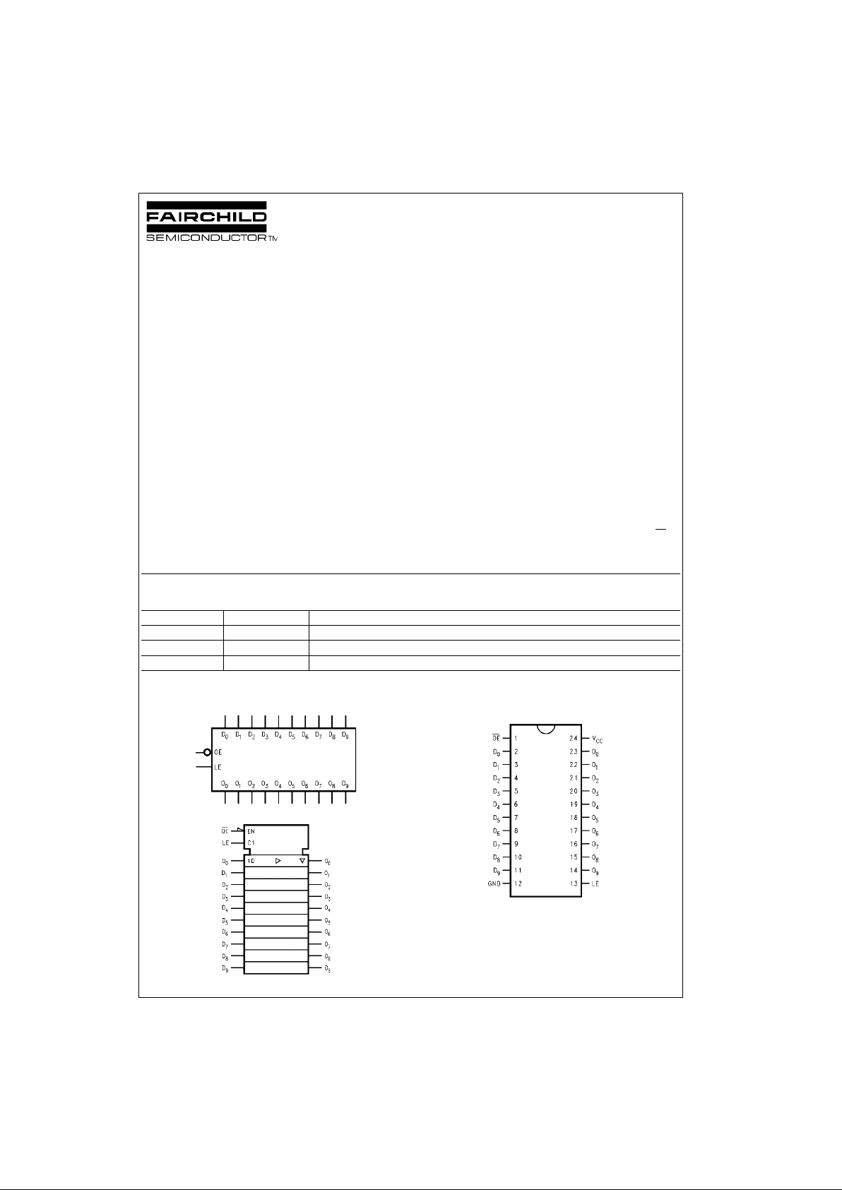
Logic Symbols
IEEE/IEC
Connection Diagram
Order Number Package Number Package Description
74LCX841WM M24B 24-Lead Small Outline Integrated Circuit (SOIC), JEDEC MS-013, 0.300” Wide
74LCX841MSA MSA24 24-Lead Shrink Small Outline Package (SSOP), EIAJ TYPE II, 5.3mm Wide
74LCX841MTC MTC24 24-Lead Thin Shrink Small Outline Package (TSSOP), JEDEC MO-153, 4.4mm Wide
www.fairchildsemi.com 2
74LCX841
Pin Descriptions Tr uth Table
H = HIGH Voltage Level
L = LOW Voltage Level
X = Immaterial
Z = High Impendance
NC = No Change
Functional Description
The LCX841 consists of ten D -type latches with 3-STATE
outputs. The flip-flops appear transparent to the data when
Latch Enable (LE) is HIGH. This allows asynchronous
operation, as the output transition follows the data in transition.
On the LE HIGH-to-LOW transition, the data that meets the
setup and hold time is latch ed. Data appears on the bus
when the Output Enable (OE
) is LOW. When OE is HIGH
the bus output is in the high impedance state.
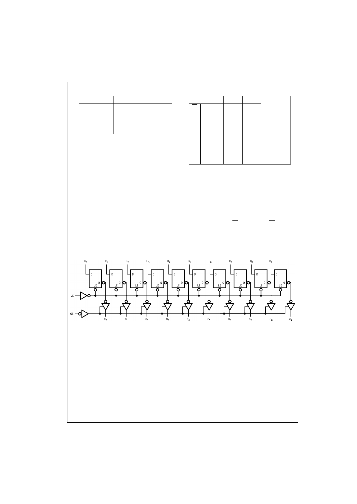
Logic Diagram
Please note that this diagram is provided o nly f or t he understanding of lo gic operations and shou ld not be used to estimate propagation delays.
Pin Names Description
D
0–D9
Data Inputs
LE Latch Enable Input
OE
Output Enable Input
O
0–O9
3-STATE Latch Outputs
Inputs Internal Output Function
OE
LE D Q O
X X X X Z High Z
H H L L Z High Z
HHH H Z High Z
H L X NC Z Latched
L H L L L Transparent
L H H H H Transparent
L L X NC NC Latched
3 www.fairchildsemi.com
74LCX841
Absolute Maximum Ratings(Note 2)
Recommended Operating Conditions (Note 4)
Note 2: The Absolute Maximum Ratings are those values beyond which the safety of the device cannot be guaranteed. The device should not be operated
at these limits. The parametric values defined in the Electrical Characteristics tables are not guaranteed at the Absolute Maximum Ratings. The “Recommended Operating C onditions” table will def ine the conditions for act ual device operation.
Note 3: I
O
Absolute Maximum Rating must be observed.
Note 4: Unused inputs must be held HIGH or LOW. They may not float.
DC Electrical Characteristics
Symbol Parameter Value Conditions Units
V
CC
Supply Voltage −0.5 to +7.0 V
V
I
DC Input Voltage −0.5 to +7.0 V
V
O
DC Output Voltage −0.5 to +7.0 Output in 3-STATE
V
−0.5 to V
CC
+ 0.5 Output in HIGH or LOW State (Note 3)
I
IK
DC Input Diode Current −50 VI < GND mA
I
OK
DC Output Diode Current −50 VO < GND mA
+50 V
O
> V
CC
I
O
DC Output Source/Sink Current ±50 mA
I
CC
DC Supply Current per Supply Pin ±100 mA
I
GND
DC Ground Current per Ground Pin ±100 mA
T
STG
Storage Temperature −65 to +150 °C
Symbol Parameter Min Max Units
V
CC
Supply Voltage Operating 2.0 3.6
V
Data Retention 1.5 3.6
V
I
Input Voltage 05.5V
V
O
Output Voltage HIGH or LOW State 0 V
CC
V
3-STATE 0 5.5
I
OH/IOL
Output Current VCC = 3.0V − 3.6V ±24
mAV
CC
= 2.7V − 3.0V ±12
V
CC
= 2.3V − 2.7V ±8
T
A
Free-Air Operating Temperature −40 85 °C
∆t/∆V Input Edge Rate, V
IN
= 0.8V − 2.0V, VCC = 3.0V 0 10 ns/V
Symbol Parameter Conditions
V
CC
TA = −40°C to +85°C
Units
(V) Min Max
V
IH
HIGH Level Input Voltage 2.3 − 2.7 1.7
V
2.7 − 3.6 2.0
V
IL
LOW Level Input Voltage 2.3 − 2.7 0.7
V
2.7 − 3.6 0.8
V
OH
HIGH Level Output Voltage IOH = −100 µA2.3 − 3.6 VCC − 0.2
V
IOH = −8 mA 2.3 1.8
IOH = −12 mA 2.7 2.2
IOH = −18 mA 3.0 2.4
IOH = −24 mA 3.0 2.2
V
OL
LOW Level Output Voltage IOH = 100 µA2.3 − 3.6 0.2
V
IOH = 8 mA 2.3 0.6
IOL = 12 mA 2.7 0.4
IOL = 16 mA 3.0 0.4
IOL = 24 mA 3.0 0.55
I
I
Input Leakage Current 0 ≤ VI ≤ 5.5V 2.3 − 3.6 ±5.0 µA
I
OZ
3-STATE Output Leakage 0 ≤ VO ≤ 5.5V 2.3 − 3.6 ±5.0
µA
VI = VIH or V
IL
I
OFF
Power-Off Leakage Current VI or VO = 5.5V 0 10 µA
 Loading...