

Fairchild Semiconductor 74LCX760 Datasheet
July 2001
Revised February 2002
74LCX760
Low Voltage Buffer/Line Driver
with 5V Tolerant Inputs and Open Drain Outputs
74LCX760 Low Voltage Buffer/Line Driver with 5V Tolerant Inputs and Open Drain Outputs
General Description
The LCX760 is the Open Drain version of the LCX244. The
LCX760 contains eight non-in verting buffers with 3 -STATE
outputs. The device may be employed as a memory
address driver, clock driver and bus-ori ented transmitter/
receiver. The LCX760 is desig ned for lo w voltage (2.5V or
3.3V) V
signal environment.
The LCX760 is fabrica ted with an advanced CMOS tech-
nology to achieve high s peed operation while maintaining
CMOS low power dissipation.
applications with capability of interfacing to a 5V
CC
Features
■ Open drai n version of the LCX244
■ 5V tolerant inputs and outputs
■ 2.3V–3.6V V
■ 8.0 ns t
■ Power down high impedance inputs and outputs
■ Supports live insertion/withdrawal (Note 1)
■ 24 mA output drive (V
■ Implements patented noise/EMI reduction circuitry
■ Latch-up conforms to JEDEC JED78
■ ESD performance:
Human body model
Machine model
Note 1: To ensure the high-impedance state during power up or down, OE
should be tied to VCC through a pull-up res istor: the m inimu m value or t he
resistor is determin ed by the current-sourc ing capability of the driver.
specifications provided
CC
max (VCC = 3.3V), 10 µA ICC max
PD
= 3.0V)
CC
> 2000V
> 200V
Ordering Code:
Order Number Package Number Package Description
74LCX760WM M20B 20-Lead Small Outline Integrated Circuit (SOIC), JEDEC MS-013, 0.300” Wide
74LCX760SJ M20D 20-Lead Small Outline Package (SOP), EIAJ TYPE II, 4.4mm Wide
74LCX760MSA MSA20 20-Lead Shrink Small Outline Package (SSOP), EIAJ TYPE II, 5.3mm Wide
74LCX760MTC MTC20 20-Lead Thin Shrink Small Outline Package (TSSOP), JEDEC MO-153, 4.4mm Wide
Devices also availab l e in Tape and Reel. Specify by appending th e s uffix let t er “X” to the ordering code.
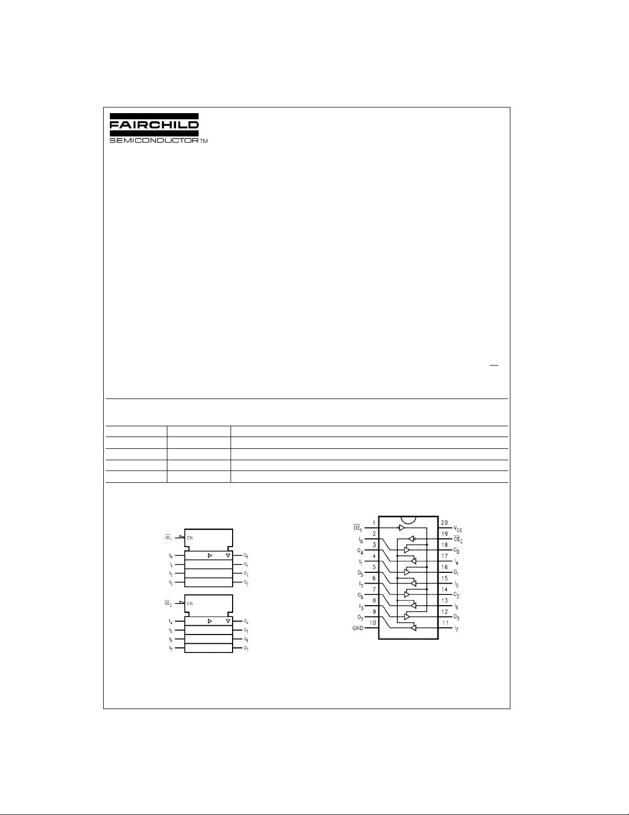
Logic Symbol
IEEE/IEC
Connection Diagram
© 2002 Fairchild Semiconductor Corporation DS500413 www.fairchildsemi.com
Pin Descriptions
74LCX760
Truth Tables
H = HIGH Voltage Level
L = LOW Voltage Level
X = Immaterial
Z = High Impedance
Pin Names Description
OE
I
0–I7
O
1
0–O7
, OE
2
3-STATE Output Enable Inputs
Inputs
Outputs
Inputs Outputs
OE
1
I
n
(Pins 12, 14, 16, 18)
LL L
LH H
HX Z
Inputs Outputs
OE
2
I
n
(Pins 3, 5, 7, 9)
LL L
LH H
HX Z
www.fairchildsemi.com 2
Absolute Maximum Ratings(Note 2)
Symbol Parameter Value Conditions Units
V
V
V
I
IK
I
OK
I
O
I
CC
I
GND
T
CC
I
O
STG
Supply Voltage −0.5 to +7.0 V
DC Input Voltage −0.5 to +7.0 V
DC Output Voltage −0.5 to +7.0 Output in HIGH or LOW Stat e (Note 3) V
DC Input Diode Current −50 VI < GND mA
DC Output Diode Current −50 VO < GND
+50 V
O
> V
CC
DC Output Sink Current 50 mA
DC Supply Current per Supply Pin ±100 mA
DC Ground Current per Ground Pin ±100 mA
Storage Temperature −65 to +150 °C
Recommended Operating Conditions (Note 4)
Symbol Parameter Min Max Units
V
CC
V
I
V
O
I
OL
T
A
∆t/∆V Input Edge Rate, V
Note 2: The Absolute Maximum Ratings are those values beyond which the safety of the device cannot be guaranteed. The device should not be operated
at these limits. The parametric values defined in the Electrical Characteristics tables are not guaranteed at the Absolute Maximum Ratings. The “Recom-
mended Operating Conditions” table will define the conditions fo r ac t ual device operation.
Note 3: I
Note 4: Unused inputs or I/Os mus t be held HIGH or LOW. They ma y n ot flo at .
Supply Voltage Operating 2.0 3.6
Data Retention 1.5 3.6
Input Voltage 0 5.5 V
Output Voltage 0 5.5 V
Output Current VCC = 3.0V − 3.6V 24
= 2.7V − 3.0V 12
CC
= 2.3V − 2.7V 8
V
CC
Free-Air Operating Temperature −40 85 °C
= 0.8V–2.0V, VCC = 3.0V 0 10 ns/V
IN
Absolute Maximum Rating must be observed.
O
V
mAV
74LCX760
mA
DC Electrical Characteristics
Symbol Parameter Conditions
V
IH
V
IL
V
OL
I
I
I
OZ
I
OFF
I
CC
∆I
CC
I
OHZ
Note 5: Outputs disabled or 3-STATE only.
HIGH Level Input Voltage 2.3 − 2.7 1.7
LOW Level Input Voltage 2.3 − 2.7 0.7
LOW Level Output Voltage IOL = 100 µA2.3 − 3.6 0.2
IOL = 8 mA 2.3 0.6
IOL = 12 mA 2.7 0.4
IOL = 16 mA 3.0 0.4
Input Leakage Current 0 ≤ VI ≤ 5.5V 2.3 − 3.6 ±5.0 µA
3-STATE Output Leakage 0 ≤ VO ≤ 5.5V
Power-Off Leakage Current VI or VO = 5.5V 0 10 µA
Quiescent Supply Current VI = VCC or GND 2.3 − 3.6 10
Increase in ICC per Input VIH = VCC −0.6V 2.3 − 3.6 500 µA
Off State Current VO = 5.5 2 - 3.6 10 µA
IOL = 24 mA 3.0 0.55
VI = VIH or V
3.6V ≤ VI, VO ≤ 5.5V (Note 5) 2.3 − 3.6 ±10
IL
3 www.fairchildsemi.com
TA = −40°C to +85°C
V
CC
(V) Min Max
2.7 − 3.6 2.0
2.7 − 3.6 0.8
2.3 − 3.6 ±5.0 µA
Units
V
V
V
µA
 Loading...