

Fairchild Semiconductor 74LCX74SJX, 74LCX74SJ, 74LCX74MX, 74LCX74MTCX, 74LCX74MTC Datasheet
...
March 1995
Revised April 1999
74LCX74 Low Voltage Dual D-Type Positive Edge-Triggered Flip-Flop with 5V Tolerant Inputs
© 1999 Fairchild Semiconductor Corporation DS012414.prf www.fairchildsemi.com
74LCX74
Low Voltage Dual D-Type Positive
Edge-Triggered Flip-Flop with 5V Tolerant Inputs
General Description
The LCX74 is a dual D-type flip-flop with Asyn chronous
Clear and Set in puts and complement ary (Q, Q
) outputs.
Information at the input is tra nsferre d to the output s on the
positive edge of the clock pulse. After the Clock Pulse input
threshold voltage has been passed, the Data input is
locked out and information present will not be transferred to
the outputs until the next rising edge of the Clock Pulse
input.
Asynchronous Inputs:
LOW input to S
D
(Set) sets Q to HIGH level
LOW input to C
D
(Clear) sets Q to LOW level
Clear and Set are independent of clock
Simultaneous LOW on C
D
and SD makes both Q and Q
HIGH
Features
■ 5V tolerant inputs
■ 2.3V–3.6V V
CC
specifications provided
■ 7.0 ns t
PD
max (V
CC
= 3.3V), 10 µA ICC max
■ Power down high impedance inputs and outputs
■ ±24 mA output drive (V
CC
= 3.0V)
■ Implements patented noise/EMI reduction circuitry
■ Latch-up performance exceeds 500 mA
■ ESD performance:
Human body model > 2000V
Machine model > 200V
Ordering Code:
Devices also availab le in Tape and Reel. Specify by appending th e s uffix let t er “X” to the ordering cod e.
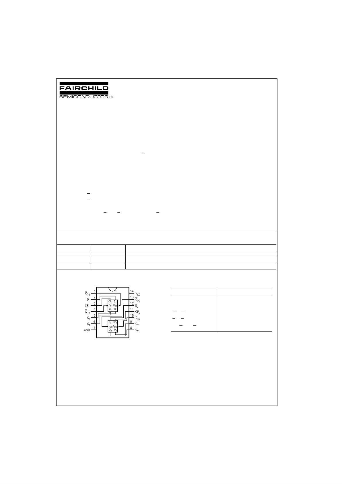
Connection Diagram Pin Descriptions
Order Number Package Number Package Description
74LCX74M M14A 14-Lead Small Outline Integrated Circuit (SOIC), JEDEC MS-120, 0.150” Narrow
74LCX74SJ M14D 14-Lead Small Outline Package (SOP), EIAJ TYPE II, 5.3mm Wide
74LCX74MTC MTC14 14-Lead Thin Shrink Small Outline Package (TSSOP), JEDEC MO-153, 4.4mm Wide
Pin Names Description
D
1
, D
2
Data Inputs
CP
1
, CP
2
Clock Pulse Inputs
C
D1
, C
D2
Direct Clear Inputs
S
D1
, S
D2
Direct Set Inputs
Q
1
, Q1, Q2, Q
2
Outputs
www.fairchildsemi.com 2
74LCX74
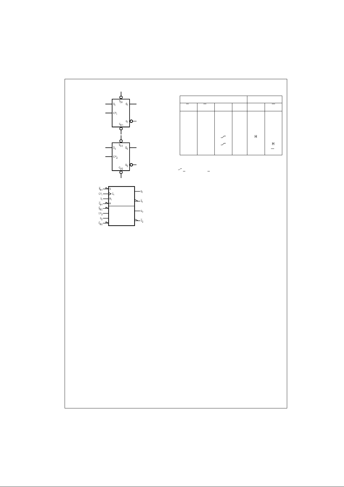
Logic Symbols
IEEE/IEC
Tr uth Table
(Each Half)
H = HIGH Voltage Level
L = LOW Voltage Level
X = Immaterial
= LOW-to-HIGH Clock Transition
Q
0(Q0
) = Previous Q(Q) before LOW-to-HIGH Transition of Clock
Inputs Outputs
S
D
C
D
CP D Q Q
LHXXHL
HLXXLH
LLXXHH
HH
HH L
HH
LLH
HHLXQ
0
Q
0
3 www.fairchildsemi.com
74LCX74
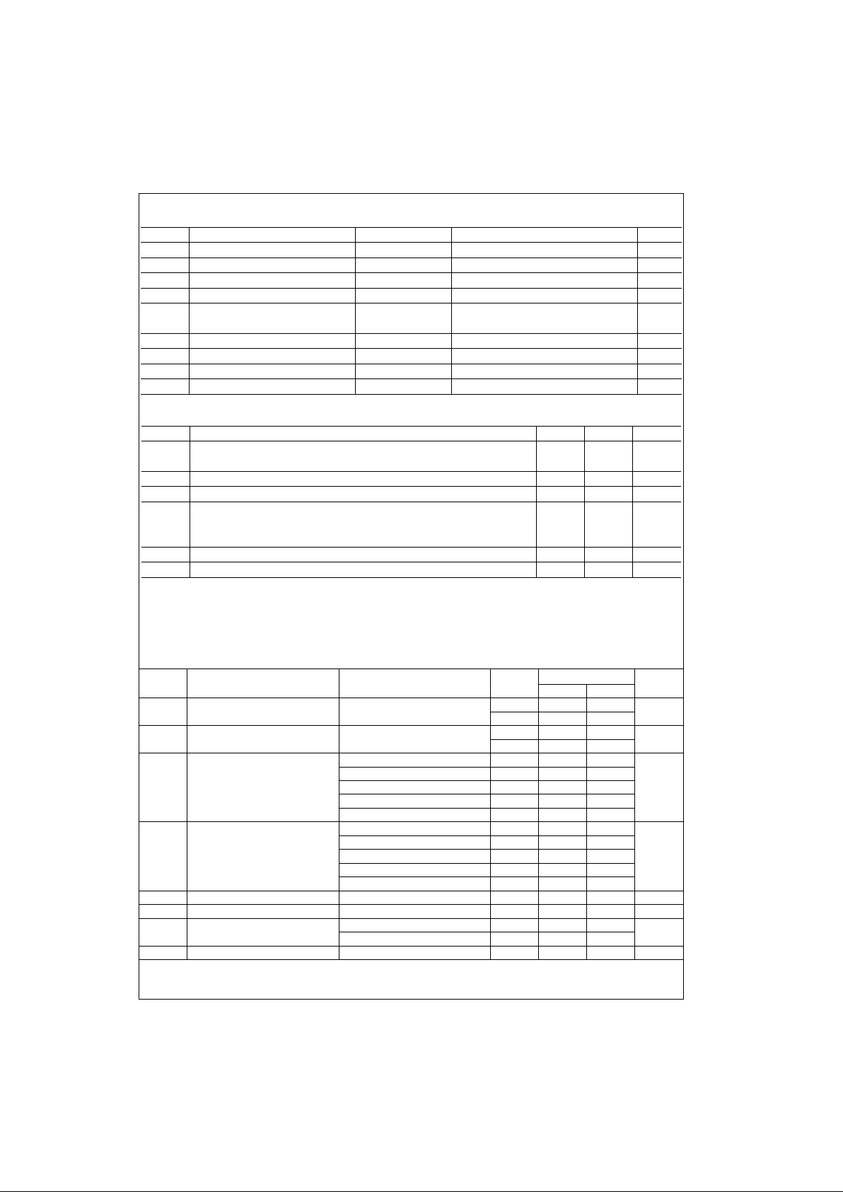
Absolute Maximum Ratings(Note 1)
Recommended Operating Conditions (Note 4)
Note 1: The Absolute Maximum Ratings are those values beyond which the safety of the device cannot be guaranteed. The device should not be operated
at these limits. The parametric values defined in the Electrical Characteristics tables are not guaranteed at the Absolute Maximum Ratings. The “Recommended Operating C onditions” table will def ine the conditions for act ual device operation.
Note 2: I
O
Absolute Maximum Rating must be observed.
Note 3: Unused inputs must be held HIGH or LOW. They may not float.
DC Electrical Characteristics
Symbol Parameter Value Conditions Units
V
CC
Supply Voltage −0.5 to +7.0 V
V
I
DC Input Voltage −0.5 to +7.0 V
V
O
DC Output Voltage −0.5 to VCC + 0.5 Output in HIGH or LOW State (Note 2) V
I
IK
DC Input Diode Current −50 VI < GND mA
I
OK
DC Output Diode Current −50 VO < GND
mA
+50 V
O
> V
CC
I
O
DC Output Source/Sink Current ±50 mA
I
CC
DC Supply Current per Supply Pin ±100 mA
I
GND
DC Ground Current per Ground Pin ±100 mA
T
STG
Storage Temperature −65 to +150 °C
Symbol Parameter Min Max Units
V
CC
Supply Voltage Operating 2.0 3.6
V
Data Retention 1.5 3.6
V
I
Input Voltage 05.5V
V
O
Output Voltage HIGH or LOW State 0 V
CC
V
I
OH/IOL
Output Current VCC = 3.0V − 3.6V ±24
mAV
CC
= 2.7V − 3.0V ±12
V
CC
= 2.3V − 2.7V ±8
T
A
Free-Air Operating Temperature −40 85 °C
∆t/∆V Input Edge Rate, V
IN
= 0.8V–2.0V, VCC = 3.0V 0 10 ns/V
Symbol Parameter Conditions
V
CC
TA = −40°C to +85°C
Units
(V) M in Max
V
IH
HIGH Level Input Voltage 2.3 − 2.7 1.7
V
2.7 − 3.6 2.0
V
IL
LOW Level Input Voltage 2.3 − 2.7 0.7
V
2.3 − 3.6 0.8
V
OH
HIGH Level Output Voltage IOH = −100µA2.3 − 3.6 VCC - 0.2
IOH = -8 mA 2.3 1.8
V
IOH = −12 mA 2.7 2.2
IOH = −18 mA 3.0 2.4
IOH = −24 mA 3.0 2.2
V
OL
LOW Level Output Voltage IOL = 100µA2.3 − 3.6 0.2
IOL = 8mA 2.3 0.6
IOL = 12 mA 2.7 0.4 V
IOL = 16 mA 3.0 0.4
IOL = 24 mA 3.0 0.55
I
I
Input Leakage Current 0 ≤ VI ≤ 5.5V 2.3 − 3.6 ±5.0 µA
I
OFF
Power-Off Leakage Current VI or VO = 5.5V 0 10 µA
I
CC
Quiescent Supply Current VI = VCC or GND 2.3 − 3.6 10
µA
3.6V ≤ VI ≤ 5.5V 2.3 − 3.6 ±10
∆I
CC
Increase in ICC per Input VIH = VCC −0.6V 2.3 − 3.6 500 µA
 Loading...