

Fairchild Semiconductor 74LCX652MSA, 74LCX652CW, 74LCX652WMX, 74LCX652WM, 74LCX652MTCX Datasheet
...
February 1994
Revised April 1999
74LCX652 Low Voltage Transceiver/Register with 5V Tolerant Inputs and Outputs
© 1999 Fairchild Semiconductor Corporation DS011998.prf www.fairchildsemi.com
74LCX652
Low Voltage Transceiver/Register with 5V Tolerant
Inputs and Outputs
General Description
The LCX652 consists of bus transceiver circuits with Dtype flip-flops, and control circuitry arranged for multiplexed
transmission of data directly from the input bus or from
internal registers. Data on the A or B bus will be clocked
into the registers a s the appropr iate clock pin g oes to the
HIGH logic level. Output Enable pins (OEAB, OEBA
) are
provided to control the transceiver function.
The LCX652 is designed for low voltage (2.5V or 3.3V) V
CC
applications with capability of interfacing to a 5V signal
environment.
The LCX652 is fabrica ted with an advanced CMOS technology to achieve high spee d operation while mai ntaining
CMOS low power dissipation.
Features
■ 5V tolerant inputs and outputs
■ 2.3V − 3.6V V
CC
specifications provided
■ 7.0 ns t
PD
max (VCC = 3.3V), 10 µA ICC max
■ Power down high impedance inputs and outputs
■ Supports live insertion/withdrawal (Note 1)
■ ±24 mA output drive (V
CC
= 3.0V)
■ Implements patented noise/EMI reduction circuitry
■ Latch-up performance exceeds 500 mA
■ ESD performance:
Human body model > 2000V
Machine model > 200V
Note 1: To ensure the high-impedan c e state during power up or down, OE
should be tied to VCC through a pull-up res istor: the m inimu m value or t he
resistor is determin ed by the current-sourcing capability of the dr iv er.
Ordering Code:
Devices also availab le in Tape and Reel. Specify by appending th e s uffix let t er “X” to the ordering cod e.
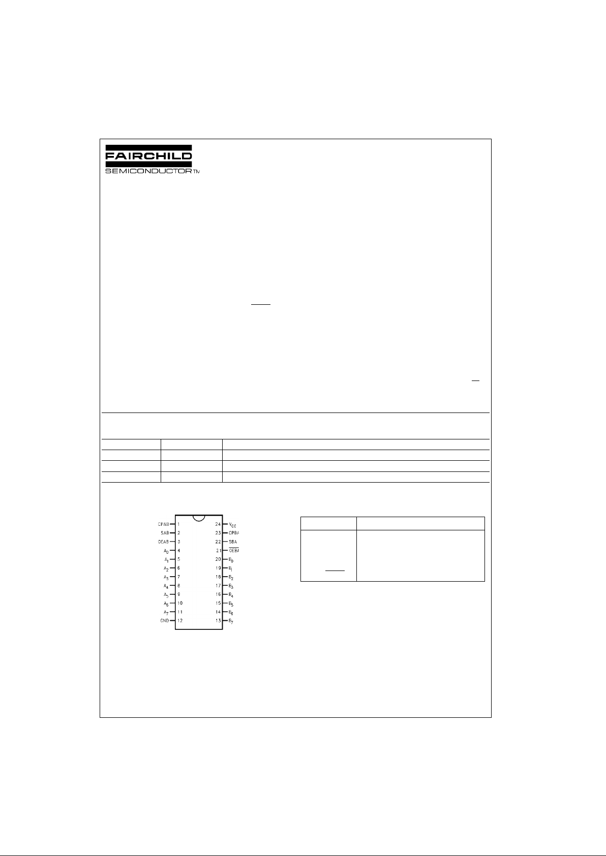
Connection Diagram Pin Descriptions
Order Number Package Number Package Description
74LCX652WM M24B 24-Lead Small Outline Integrated Circuit (SOIC), JEDEC MS-013, 0.300” Wide
74LCX652MSA MSA24 24-Lead Shrink Small Outline Package (SSOP), EIAJ TYPE II, 5.3mm Wide
74LCX652MTC MTC24 24-Lead Thin Shrink Small Outline Package (TSSOP), JEDEC MO-153, 4.4mm Wide
Pin Names Description
A
0–A7
, B0–B7A and B Inputs/3-STATE Outputs
CPAB, CPBA Clock Inputs
SAB, SBA Select Inputs
OEAB, OEBA
Output Enable Inputs
www.fairchildsemi.com 2
74LCX652
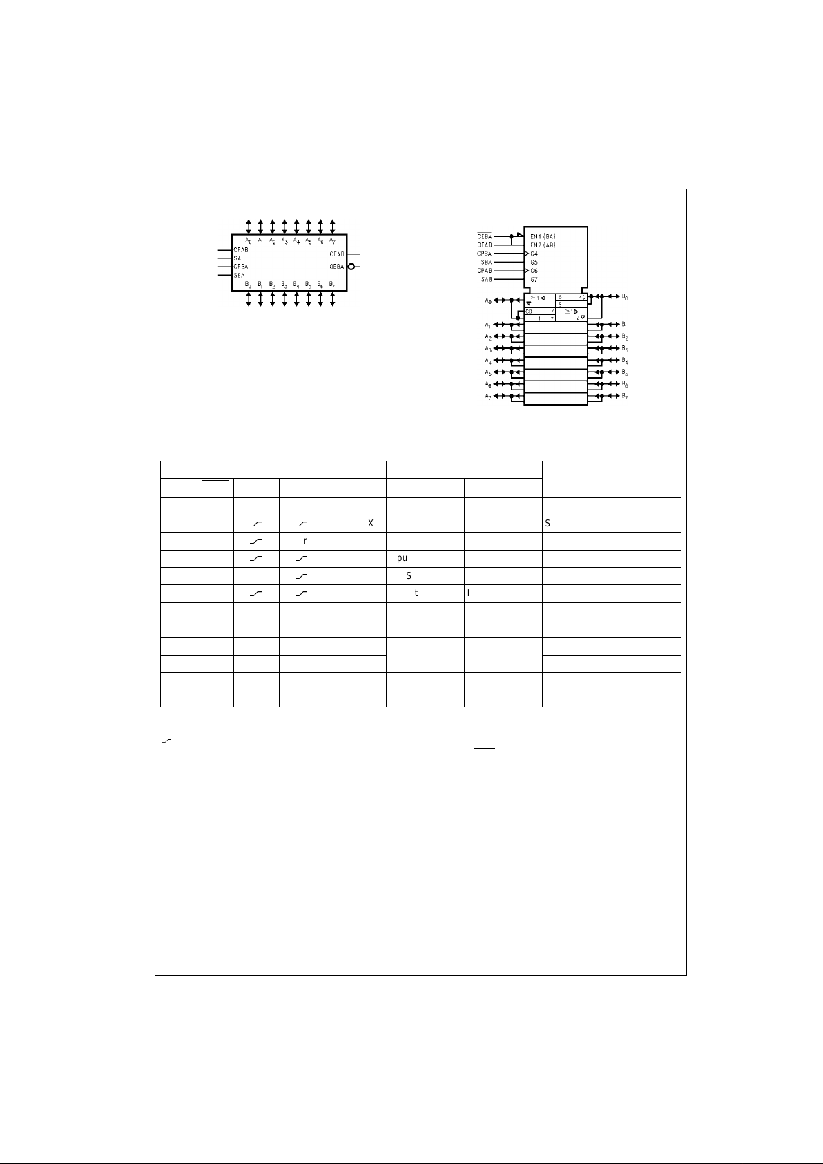
Logic Symbols
IEEE/IEC
Truth Table
(Note 2)
H = HIGH Voltage Level
L = LOW Voltage Level
X = Immaterial
= LOW-to-HIGH Clock Transition
Note 2: The data output fu nction s may b e enable d or di sabled b y variou s signa ls at OEA B or O EBA
inputs. Data input function s are a lways e nabled, i.e.,
data at the bus pins w ill be stored on every LOW- to -H I GH t ransition on the clock inputs.
Inputs Inputs/Outputs Operating Mode
OEAB OEBA
CPAB CPBA SAB SBA A0 thru A
7
B0 thru B
7
L H H or L H or L X X Input Input Isolation
LH
X X Store A and B Data
XH
H or L X X Input Not Specified Store A, Hold B
HH
X X Input Output Store A in Both Registers
LXH or L
X X Not Specified Input Hold A, Store B
LL
X X Output Input Store B in Both Registers
L L X X X L Output Input Real-Time B Data to A Bus
L L X H or L X H Store B Data to A Bus
H H X X L X Input Output Real-Time A Data to B Bus
H H H or L X H X Stored A Data to B Bus
H L H or L H or L H H Output Output Stored A Data to B Bus and
Stored B Data to A Bus
3 www.fairchildsemi.com
74LCX652
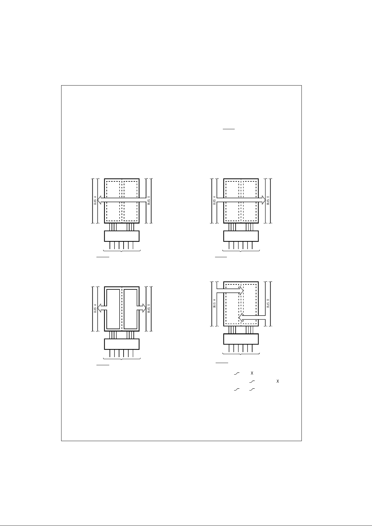
Functional Description
In the transceiver mode , data present a t the HIGH impe dance port may be sto red in either the A or B register or
both.
The select (SAB, SBA) controls can multiplex stored and
real-time.
The examples below demonstrate the four fundamental
bus-management fun cti on s t hat c an be performed w ith t he
Octal bus transceiver and receiver.
Data on the A or B data bus, or both can be stored in the
internal D flip-flop by LOW to HIGH transitions at the
appropriate Clock Inp uts (CPAB, CPBA) regardless of the
Select or Output Enable Inputs. When SAB and SBA are in
the real time transfer m od e, it is a lso po ssibl e to sto re d ata
without using the internal D flip-flops by simultaneously
enabling OEAB and OEBA
. In this configuration each Output reinforces its Input. Thus when all other data sources to
the two sets of bus lines a re in a HIGH impedance state ,
each set of bus lines will remain at its last state.
Real-Time Transfer
Bus B to Bus A
Transfer Storage
Data to A or B
Real-Time Transfer
Bus A to Bus B
Storage
OEAB OEBA
CPAB CPBA SAB SBA
LLXXXL
OEAB OEBA
CPAB CPBA SAB SBA
H L H or L H or L H H
OEAB OEBA CPAB CPBA SAB SBA
HHXXLX
OEAB OEBA
CPAB CPBA SAB SBA
XH
XXX
LXX
XX
LH
XX
 Loading...