

Fairchild Semiconductor 74LCX646WMX, 74LCX646WM, 74LCX646MTCX, 74LCX646MTC, 74LCX646MSAX Datasheet
...
February 1994
Revised April 1999
74LCX646 Low Voltage Octal Transceiver/Register with 5V Toler ant Inputs and Outputs
© 1999 Fairchild Semiconductor Corporation DS011997.prf www.fairchildsemi.com
74LCX646
Low Voltage Octal Transceiver/Register with 5V Tolerant
Inputs and Outputs
General Description
The LCX646 consists of registered bus transceiver circuits,
D-type flip-flops, and control circuitry providing multiplexed
transmission of data d irectly from the in put b us or fr om the
internal storage registers. Data on the A or B bus will be
loaded into the respective registers on the LOW-to-HIGH
transition of the appropriate pin (CPAB or CPBA)(see
Functional Description).
The LCX646 is designed for low voltage (2.5V or 3.3V) V
CC
applications with capability of interfacing to a 5V signal
environment.
The LCX646 is fabrica ted with an advanced CMOS technology to achieve high spee d operation while mai ntaining
CMOS low power dissipation.
Features
■ 5V tolerant inputs and outputs
■ 2.3V − 3.6V V
CC
specifications provided
■ 7.0 ns t
PD
max (VCC = 3.3V), 10 µA ICC max
■ Power down high impedance inputs and outputs
■ Supports live insertion/withdrawal (Note 1)
■ ±24 mA output drive (V
CC
= 3.0V)
■ Implements patented noise/EMI reduction circuitry
■ Latch-up performance exceeds 500 mA
■ ESD performance:
Human body model > 2000V
Machine model > 200V
Note 1: To ensure the high-impedan c e state during power up or down, OE
should be tied to VCC through a pull-up res istor: the m inimu m value or t he
resistor is determin ed by the current-sourcing capability of the dr iv er.
Ordering Code:
Devices also availab le in Tape and Reel. Specify by appending th e s uffix let t er “X” to the ordering code.
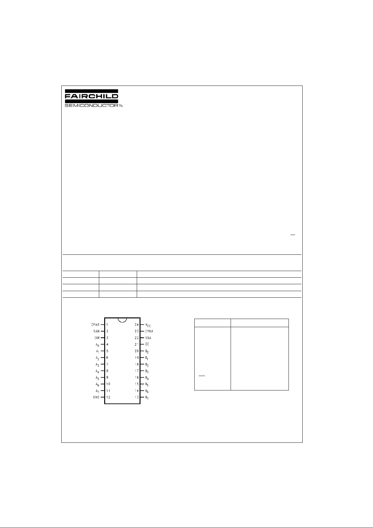
Connection Diagram Pin Descriptions
Order Number Package Number Package Description
74LCX646WM M24B 24-Lead Small Outline Integrated Circuit (SOIC), JEDEC MS-013, 0.300” Wide
74LCX646MSA MSA24 24-Lead Shrink Small Outline Package (SSOP), EIAJ TYPE II, 5.3mm Wide
74LCX646MTC MTC24 24-Lead Thin Shrink Small Outline Package (TSSOP), JEDEC MO-153, 4.4mm Wide
Pin Names Description
A
0–A7
Data Register A Inputs
Data Register A Outputs
B
0–B7
Data Register B Inputs
Data Register B Outputs
CPAB, CPBA Clock Pulse Inputs
SAB, SBA Transmit/Receive Inputs
OE
Output Enable Input
DIR Direction Control Input
www.fairchildsemi.com 2
74LCX646
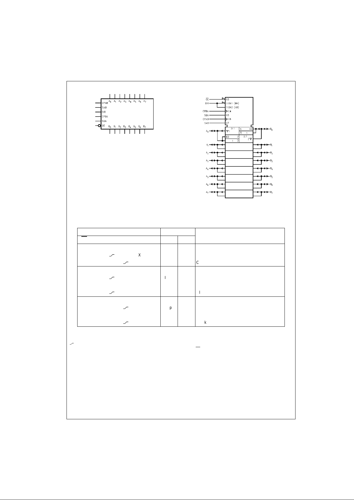
Logic Symbols
IEEE/IEC
Truth Table
(Note 2)
H = HIGH Voltage Level
L = LOW Voltage Level
X = Immaterial
= LOW-to-HIGH Transitio n
Note 2: The data o utput fu nctions may be en abled or disabl ed by vario us sig nals at th e OE
and DIR inputs. Data input functions are always enabled; i.e.,
data at the bus pins w ill be stored on every LOW- to -H I GH t ransition of the appropriate clock inputs.
Inputs Data I/O Function
OE
DIR CPAB CPBA SAB SBA A0–A7B0–B
7
H X H or L H or L X X Isolation
HX
X X X Input Input Clock An Data into A Register
HXX
X X Clock Bn Data into B Register
LHXXLX A
n
to Bn—Real Time (Transparent Mode)
LH
X L X Input Output Clock An Data into A Register
L H H or L X H X A Register to B
n
(Stored Mode)
LH
X H X Clock An Data into A Register and Output to B
n
LLXXXL Bn to An—Real Time (Transparent Mode)
LLX
X L Output Input Clock Bn Data into B Register
L L X H or L X H B Register to A
n
(Stored Mode)
LLX
X H Clock Bn Data into B Register and Output to A
n

3 www.fairchildsemi.com
74LCX646
Functional Description
In the transceiver mode , data present a t the HIGH impe dance port may be sto red in either the A or B register or
both. The select (SAB, SBA) controls can multiplex stored
and real-time. The examples shown below demonstrate the
four fundamental bus-m anagement functions that can be
performed.
The direction control (DIR) determines which bus will
receive data when OE
is LOW. In the isolation mode (OE
HIGH), A data may be stored in one reg ister and /or B data
may be stored in the other re gister. When an ou tput function is disabled, the input fu nction is still e nabled and may
be used to store and tr ansmit data. Only one of the two
busses, A or B, may be driven at a time.
Real-Time Transfer
Bus B to Bus A
Real-Time Transfer
Bus A to Bus B
Transfer Storage
Data to A or B
Storage
OE
DIR CPAB CPBA SAB SBA
LL X X X L
OE DIR CPAB CPBA SAB SBA
LHXXLX
OE DIR CPAB CPBA SAB SBA
LLXH or LX H
LHH or LXHX
OE DIR CPAB CPBA SAB SBA
LH
XLX
LLX
XL
HX
XXX
HXX
XX
 Loading...