

Fairchild Semiconductor 74LCX573WMX, 74LCX573WM, 74LCX573SJX, 74LCX573SJ, 74LCX573MTCX Datasheet
...
March 1995
Revised April 1999
74LCX573 Low Voltage Octal Latch with 5V Tolerant Inputs and Outputs
© 1999 Fairchild Semiconductor Corporation DS012405.prf www.fairchildsemi.com
74LCX573
Low Voltage Octal Latch with 5V Tolerant
Inputs and Outputs
General Description
The LCX573 is a high-speed octal latch with buff ere d com mon Latch Enable (LE) and buffered common Output
Enable (OE
) inputs.
The LCX573 is functionally identical to the LCX373 but has
inputs and outputs on opposite sides.
The LCX573 is designed for low voltage (3.3V or 2.5V)
applications with capability of interfacing to a 5V signal
environment. The LCX57 3 is fabricated with an advanc ed
CMOS technology to achieve high speed operation while
maintaining CMOS low power dissipation.
Features
■ 5V tolerant inputs and outputs
■ 2.3V–3.6V V
CC
specifications provided
■ 7.0 ns t
PD
max (VCC = 3.3V), 10 µA ICC max
■ Power down high impedance inputs and outputs
■ Supports live insertion/withdrawal (Note 1)
■ ±24 mA output drive (V
CC
= 3.0V)
■ Implements patented noise/EMI reduction circuitry
■ Latch-up performance exceeds 500 mA
■ ESD performance:
Human body model > 2000V
Machine model > 200V
Note 1: To ensure the high-impedan c e state during power up or down, OE
should be tied to VCC through a pull-up res istor: the m inimu m value or t he
resistor is determin ed by the current-sourcing capability of the dr iv er.
Ordering Code:
Devices also availab le in Tape and Reel. Specify by appending th e s uffix let t er “X” to the ordering code.
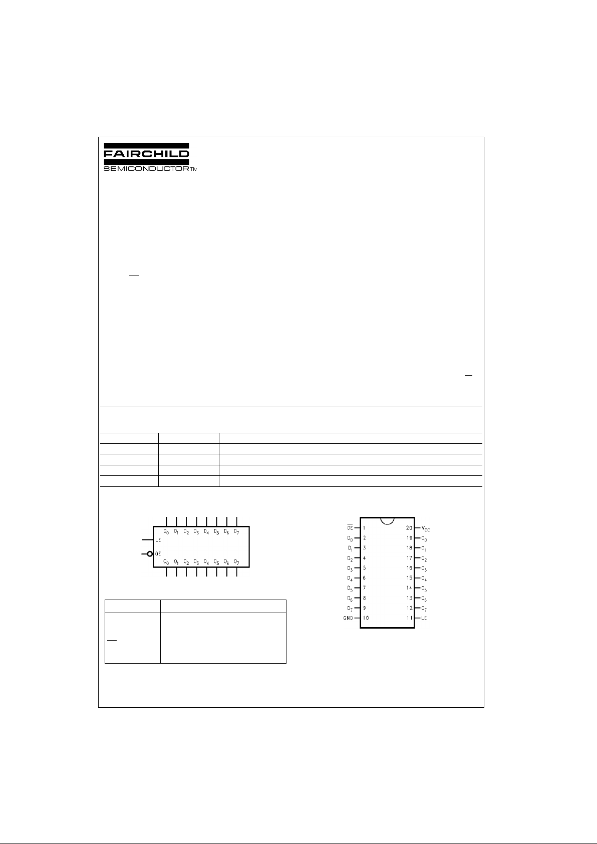
Logic Symbol
Pin Descriptions
Connection Diagram
Order Number Package Number Package Description
74LCX573WM M20B 20-Lead Small Outline Integrated Circuit (SOIC), JEDEC MS-013, 0.300” Wide
74LCX573SJ M20D 20-Lead Molded Small Outline (SOP), EIAJ TYPE II, 5.3mm Wide
74LCX573MSA MSA20 20-Lead Shrink Small Outline Package (SSOP), EIAJ TYPE II, 5.3mm Wide
74LCX573MTC MTC20 20-Lead Thin Shrink Small Outline Package (TSSOP), JEDEC MO-153, 4.4mm Wide
Pin Names Description
D
0–D7
Data Inputs
LE Latch Enable Input
OE
3-STATE Output Enable Input
O
0–O7
3-STATE Latch Outputs
www.fairchildsemi.com 2
74LCX573
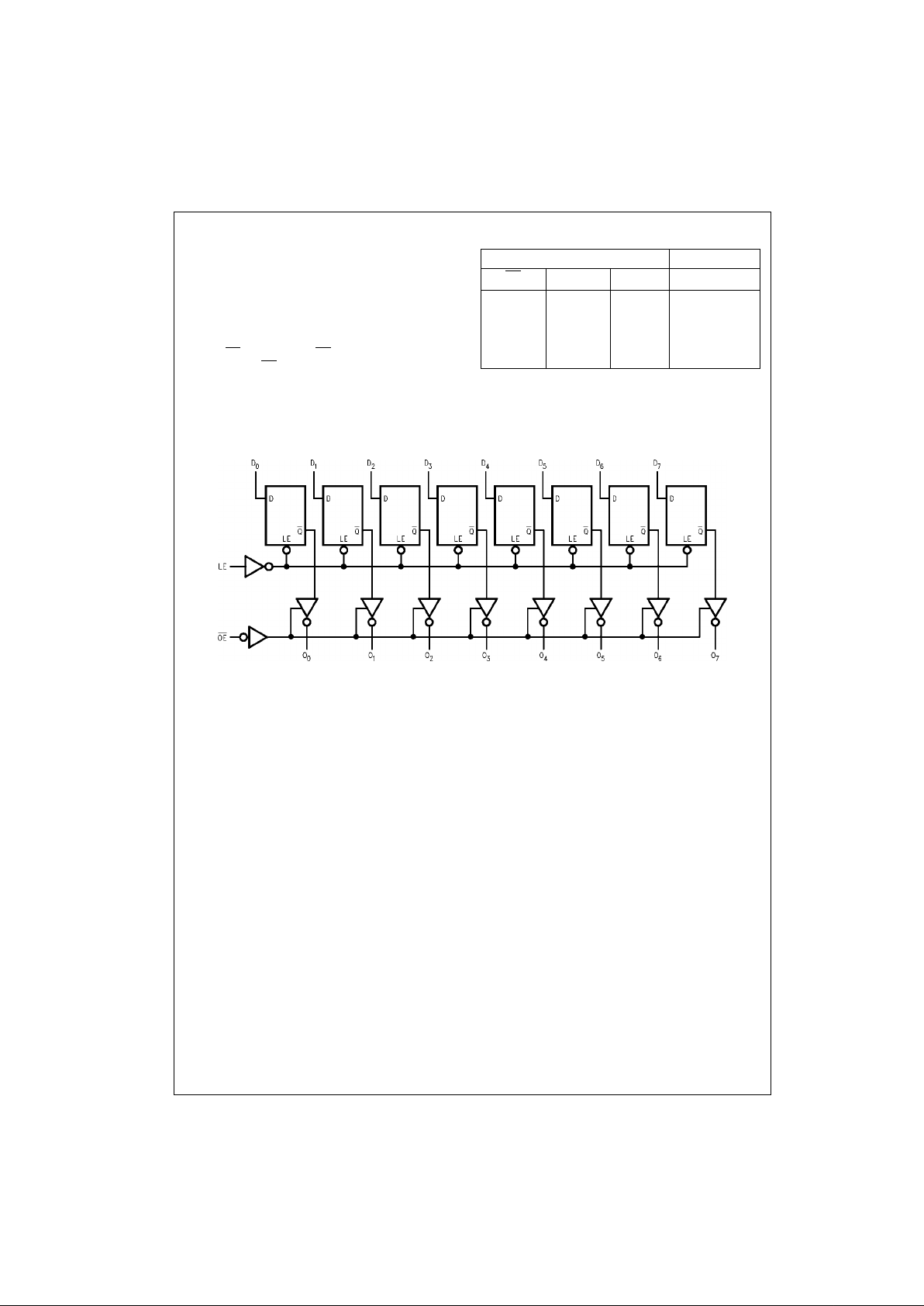
Functional Description
The LCX573 contains eig ht D-type latches with 3-STATE
output buffers. When the La tch En able ( LE) inpu t is HI GH,
data on the D
n
inputs enters the latches. In this co ndition
the latches are transparent, i.e., a latch output will chang e
state each time its D input ch anges. Whe n LE is L OW the
latches store the information that was present on th e D
inputs a setup time preceding the HIGH-to-LOW transitio n
of LE. The 3-STATE buffers are controlled by the O utput
Enable (OE
) input. When OE is LOW, the buffers are
enabled. When OE
is HIGH the buffers are in the high
impedance mode but this does not interfere with entering
new data into the latches.
Tr uth Table
H = HIGH Voltage
L = LOW Voltage
Z = High Impedance
X = Immaterial
O
0
= Previous O0 before HIGH-to-LOW transition of Latch Enable
Logic Diagram
Please note that this diagram is provided o nly f or t he understanding of lo gic operations and should not be used to estimate propagation delays.
Inputs Outputs
OE
LE D O
n
LHH H
LHL L
LLX O
0
HXX Z
3 www.fairchildsemi.com
74LCX573
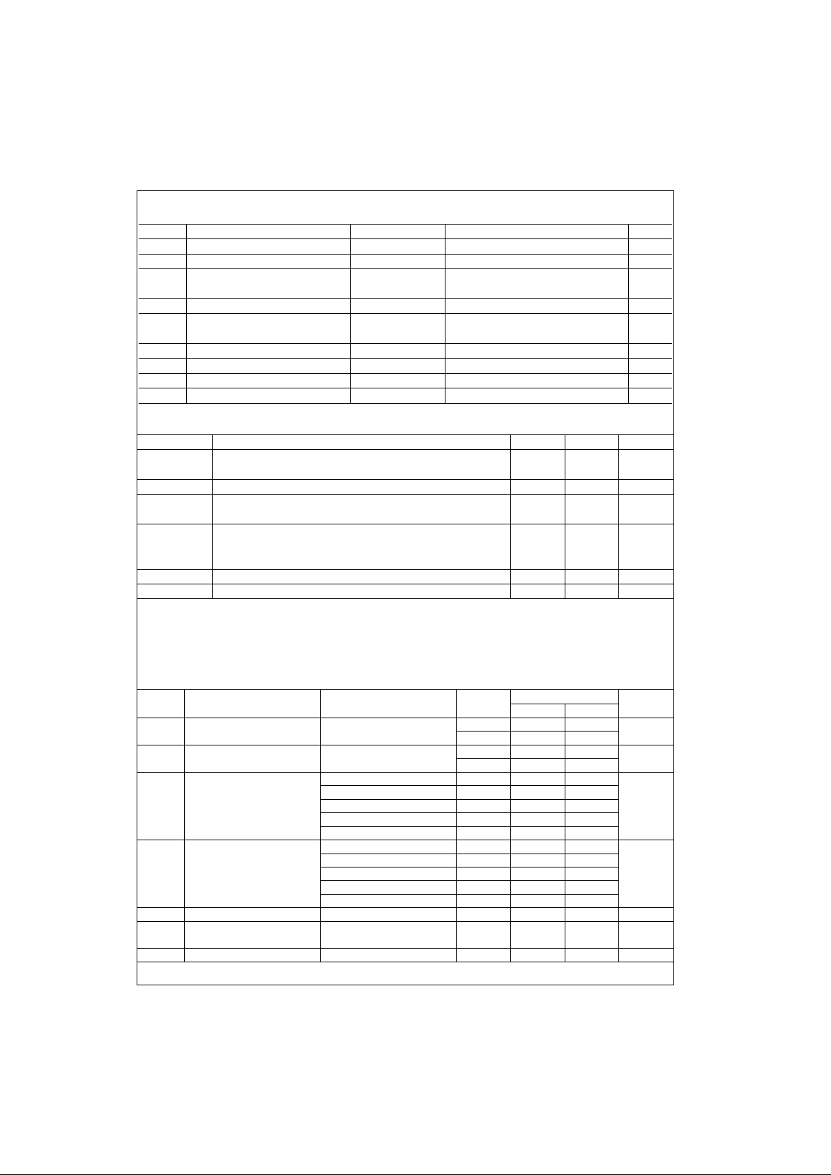
Absolute Maximum Ratings(Note 2)
Recommended Operating Conditions (Note 4)
Note 2: The Absolute Maximum Ratings are those values beyond which the safety of the device cannot be guaranteed. The device should not be operated
at these limits. The parametric values defined in the Electrical Characteristics tables are not guaranteed at the Absolute Maximum Ratings. The “Recommended Operating C onditions” table will def ine the conditions for act ual device operation.
Note 3: I
O
Absolute Maximum Rating must be observed.
Note 4: Unused (inputs or I/O's) must be held HIGH or LOW. They may not float.
DC Electrical Characteristics
Symbol Parameter Value Conditions Units
V
CC
Supply Voltage −0.5 to +7.0 V
V
I
DC Input Voltage −0.5 to +7.0 V
V
O
DC Output Voltage −0.5 to +7.0 Output in 3-STATE V
−0.5 to V
CC
+ 0.5 Output in HIGH or LOW State (Note 3)
I
IK
DC Input Diode Current −50 VI < GND mA
I
OK
DC Output Diode Current −50 VO < GND
mA
+50 V
O
> V
CC
I
O
DC Output Source/Sink Current ±50 mA
I
CC
DC Supply Current per Supply Pin ±100 mA
I
GND
DC Ground Current per Ground Pin ±100 mA
T
STG
Storage Temperature −65 to +150 °C
Symbol Parameter Min Max Units
V
CC
Supply Voltage Operating 2.0 3.6
V
Data Retention 1.5 3.6
V
I
Input Voltage 0 5.5 V
V
O
Output Voltage HIGH or LOW State 0 V
CC
V
3-STATE 0 5.5
I
OH/IOL
Output Current VCC = 3.0V − 3.6V ±24
mAV
CC
= 2.7V − 3.0V ±12
V
CC
= 2.3V − 2.7V ±8
T
A
Free-Air Operating Temperature −40 85 °C
∆t/∆V Input Edge Rate, V
IN
= 0.8V − 2.0V, VCC = 3.0V 0 10 ns/V
Symbol Parameter Conditions
V
CC
TA = −40°C to +85°C
Units
(V) Min Max
V
IH
HIGH Level Input Voltage 2.3 − 2.7 1.7
V
2.7 − 3.6 2.0
V
IL
LOW Level Input Voltage 2.3 − 2.7 0.7
V
2.7 − 3.6 0.8
V
OH
HIGH Level Output Voltage IOH = −100 µA2.3 − 3.6 VCC − 0.2
V
IOH = −8 mA 2.3 1.8
IOH = −12 mA 2.7 2.2
IOH = −18 mA 3.0 2.4
IOH = −24 mA 3.0 2.2
V
OL
LOW Level Output Voltage IOL = 100 µA2.3 − 3.6 0.2
V
IOL = 8 mA 2.3 0.6
IOL = 12 mA 2.7 0.4
IOL = 16 mA 3.0 0.4
IOL = 24 mA 3.0 0.55
I
I
Input Leakage Current 0 ≤ VI ≤ 5.5V 2.3 − 3.6 ±5.0 µA
I
OZ
3-STATE Output Leakage 0 ≤ VO ≤ 5.5V 2.3 − 3.6 ±5.0
µA
VI = VIH or V
IL
I
OFF
Power-Off Leakage Current VI or VO = 5.5V 0 10 µA
 Loading...