

Fairchild Semiconductor 74LCX543CW, 74LCX543WMX, 74LCX543WM, 74LCX543MTCX, 74LCX543MTC Datasheet
...
May 1995
Revised April 1999
74LCX543 Low Voltage Octal Registered Transceiver with 5V Tolerant Inputs and Outputs
© 1999 Fairchild Semiconductor Corporation DS012463.prf www.fairchildsemi.com
74LCX543
Low Voltage Octal Registered Transceiver with
5V Tolerant Inputs and Outputs
General Description
The LCX543 is a n on- inve rtin g octal transceiver contai n ing
two sets of D-type register s for temporary storage o f data
flowing in either direction. Separate Latch Enable and Output Enable inputs are provided for each register to permit
independent input and output control in either direction of
data flow.
The LCX543 is designed for low voltage (2.5V or 3.3V) V
CC
applications with capability of interfacing to a 5V signal
environment.
The LCX543 is fabrica ted with an advanced CMOS technology to achieve high spee d operation while mai ntaining
CMOS low power dissipation.
Features
■ 5V tolerant inputs and outputs
■ 2.3V − 3.6V V
CC
specifications provided
■ 7.0 ns t
PD
max (VCC = 3.3V), 10 µA ICC max
■ Power down high impedance inputs and outputs
■ Supports live insertion/withdrawal (Note 1)
■ ±24 mA Output Drive (V
CC
= 3.0V)
■ Implements patented noise/EMI reduction circuitry
■ Latch-up performance exceeds 500 mA
■ ESD performance:
Human body model > 2000V
Machine model > 200V
Note 1: To ensure the high-impedan c e state during power up or do w n, OE
should be tied to VCC through a pull-up res istor: the m inimu m value or t he
resistor is determin ed by the current-sourcin g c apability of the driver.
Ordering Code:
Devices also availab le in Tape and Reel. Specify by appending th e s uffix let t er “X” to the ordering code.
Connection Diagram Pin Descriptions
Order Number Package Number Package Description
74LCX543WM M24B 24-Lead Small Outline Integrated Circuit (SOIC), JEDEC MS-013, 0.300” Wide
74LCX543MSA MSA24 24-Lead Shrink Small Outline Package (SSOP), EIAJ TYPE II, 5.3mm Wide
74LCX543MTC MTC24 24-Lead Thin Shrink Small Outline Package (TSSOP), JEDEC MO-153, 4.4mm Wide
Pin Names Description
OEAB
A-to-B Output Enable Input (Active LOW)
OEBA
B-to-A Output Enable Input (Active LOW)
CEAB
A-to-B Enable Input (Active LOW)
CEBA
B-to-A Enable Input (Active LOW)
LEAB
A-to-B Latch Enable Input (Active LOW)
LEBA
B-to-A Latch Enable Input (Active LOW)
A
0–A7
A-to-B Data Inputs or
B-to-A 3-STATE Outputs
B
0–B7
B-to-A Data Inputs or
A-to-B 3-STATE Outputs

www.fairchildsemi.com 2
74LCX543
Logic Symbols
IEEE/IEC
Data I/O Control Table
H = HIGH Voltage Level
L = LOW Voltage Level
X = Immaterial
A-to-B data flow shown ; B-to-A flow control is the same, except using
CEBA
, LEBA and OEBA
Functional Description
The LCX543 contains two sets of eight D-type latches, with
separate input and output co ntrols for each set. For data
flow from A to B, for example, th e A-to-B Enable (CEAB
)
input must be LOW in order to ent er data from A
0–A7
or
take data from B
0–B7
, as indicated in the Data I/ O Control
Ta b l e. With CEAB
LOW, a LOW signal on the A-to-B La tch
Enable (LEAB
) input makes the A-to-B latches transparent;
a subsequent LOW-to-HIGH transi tion of the LEAB
signal
puts the A latches in the storage mode and their outputs no
longer change with the A inputs. With CEAB
and OEAB
both LOW, the 3-STATE B output buffers are acti ve and
reflect the data present at the output of the A latches. Control of data flow from B to A is similar, but using the CEBA
,
LEBA
and OEBA inputs.
Logic Diagram
Please note that this diagram is provided only f or t he understanding of logic operations and should not be used to estimate propagation delays.
Inputs Latch Status Output Buffers
CEAB
LEAB OEAB
H X X Latched High Z
X H X Latched —
L L X Transparent —
X X H — High Z
L X L — Driving
3 www.fairchildsemi.com
74LCX543
Absolute Maximum Ratings(Note 2)
Recommended Operating Conditions (Note 4)
Note 2: The Absolute Maximum Ratings are those values beyond which the safety of the device cannot be guaranteed. The device should not be operated
at these limits. The parametric values defined in the Electrical Characteristics tables are not guaranteed at the Absolute Maximum Ratings. The “Recommended Operating C onditions” table will define the conditions for actua l dev ic e operation.
Note 3: I
O
Absolute Maximum Rating must be observed.
Note 4: Unused inputs or I/O's must be held HIGH or LOW. They may not float.
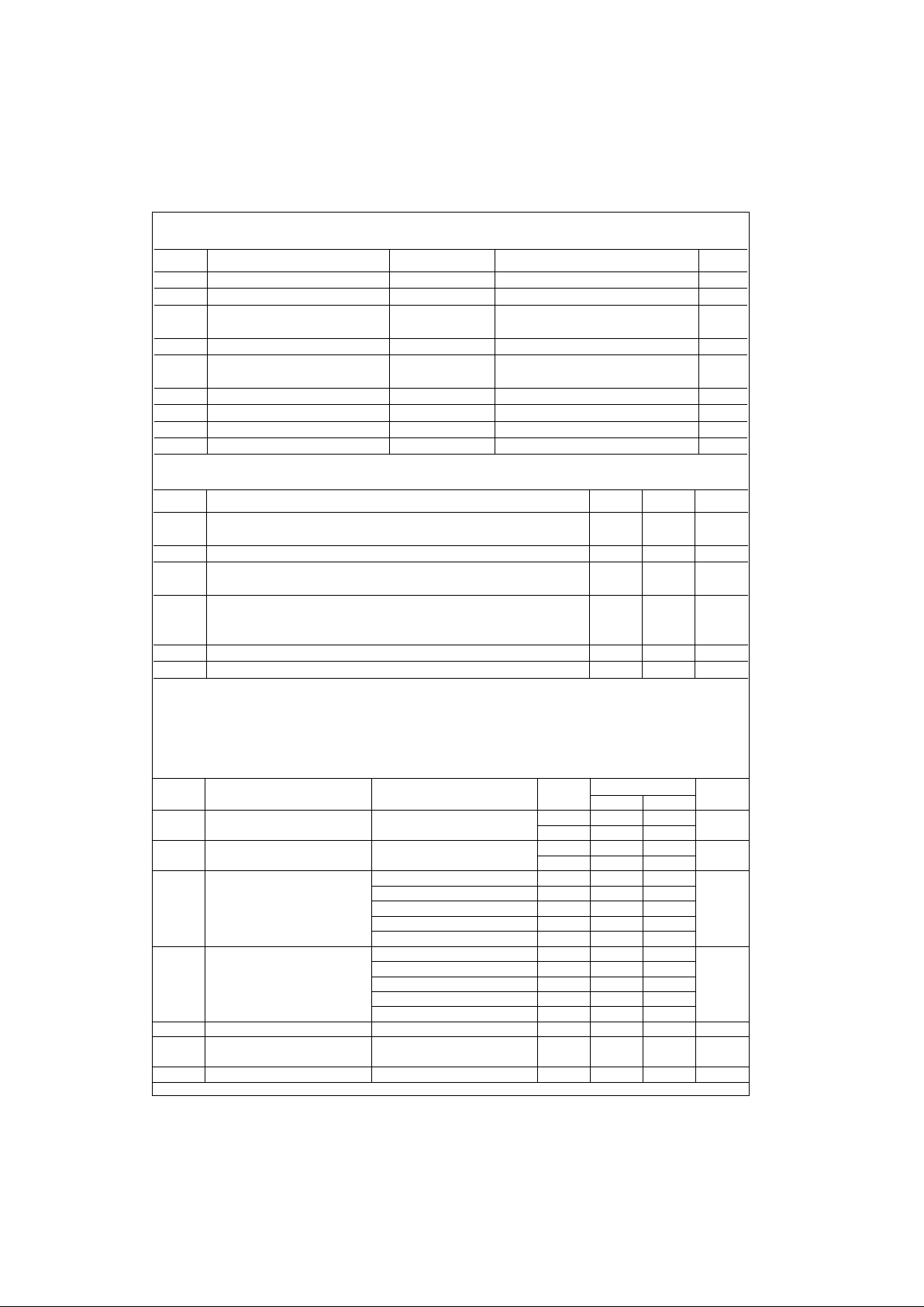
DC Electrical Characteristics
Symbol Parameter Value Conditions Units
V
CC
Supply Voltage −0.5 to +7.0 V
V
I
DC Input Voltage −0.5 to +7.0 V
V
O
DC Output Voltage −0.5 to +7.0 Output in 3-STATE
V
−0.5 to V
CC
+ 0.5 Output in HIGH or LOW State (Note 3)
I
IK
DC Input Diode Current −50 VI < GND mA
I
OK
DC Output Diode Current −50 VO < GND
mA
+50 V
O
> V
CC
I
O
DC Output Source/Sink Current ±50 mA
I
CC
DC Supply Current per Supply Pin ±100 mA
I
GND
DC Ground Current per Ground Pin ±100 mA
T
STG
Storage Temperature −65 to +150 °C
Symbol Parameter Min Max Units
V
CC
Supply Voltage Operating 2.0 3.6
V
Data Retention 1.5 3.6
V
I
Input Voltage 05.5V
V
O
Output Voltage HIGH or LOW State 0 V
CC
V
3-STATE 0 5.5
I
OH/IOL
Output Current VCC = 3.0V − 3.6V ±24
mAV
CC
= 2.7V − 3.0V ±12
V
CC
= 2.3V − 2.7V ±8
T
A
Free-Air Operating Temperature −40 85 °C
∆t/∆V Input Edge Rate, V
IN
= 0.8V − 2.0V, VCC = 3.0V 0 10 ns/V
Symbol Parameter Conditions
V
CC
TA = −40°C to +85°C
Units
(V) Min Max
V
IH
HIGH Level Input Voltage 2.3 − 2.7 1.7
V
2.7 − 3.6 2.0
V
IL
LOW Level Input Voltage 2.3 − 2.7 0.7
V
2.7 − 3.6 0.8
V
OH
HIGH Level Output Voltage IOH = −100 µA2.3 − 3.6 VCC − 0.2
V
IOH = −8 mA 2.3 1.8
IOH = −12 mA 2.7 2.2
IOH = −18 mA 3.0 2.4
IOH = −24 mA 3.0 2.2
V
OL
LOW Level Output Voltage IOL = 100 µA2.3 − 3.6 0.2
V
IOL = 8mA 2.3 0.6
IOL = 12 mA 2.7 0.4
IOL = 16 mA 3.0 0.4
IOL = 24 mA 3.0 0.55
I
I
Input Leakage Current 0 ≤ VI ≤ 5.5V 2.3 − 3.6 ±5.0 µA
I
OZ
3-STATE I/O Leakage 0 ≤ VO ≤ 5.5V 2.3 − 3.6 ±5.0
µA
VI = VIH or V
IL
I
OFF
Power-Off Leakage Current VI or VO = 5.5V 0 10 µA
 Loading...