

Fairchild Semiconductor 74LCX38MTC, 74LCX38M, 74LCX38CW, 74LCX38SJX, 74LCX38SJ Datasheet
...
© 1999 Fairchild Semiconductor Corporation DS012574 www.fairchildsemi.com
October 1995
Revised June 1999
74LCX38 Low Voltage Quad 2-Input NAND Gate (Open Drain) with 5V Tolerant Inputs
74LCX38
Low Voltage Quad 2-Input NAND Gate (Open Drain)
with 5V Tolerant Inputs
General Description
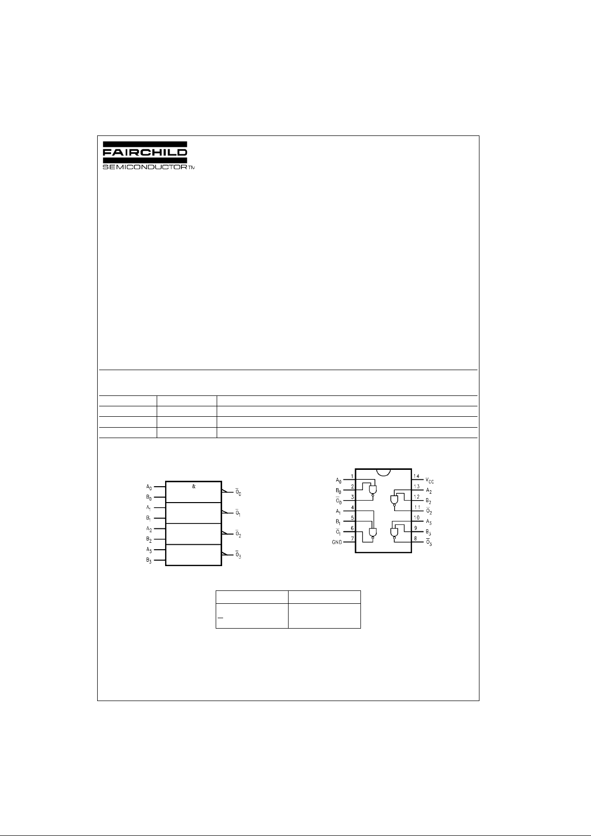
The LCX38 contains fo ur 2-input open drain NA ND gates.
The inputs tolerate voltages up to 7V allowing the interface
of 5V systems to 3V systems.
The 74LCX38 is fabricated with advanced CMO S technology to achieve high speed operation while maintaining
CMOS low power dissipation.
Features
■ 5V tolerant inputs
■ 2.3V–3.6V V
CC
specifications provided
■ 6.5 ns t
PD
max (VCC = 3.3V), 10 µA ICC max
■ Power down high impedance inputs and outputs
■ ±24 mA output drive (V
CC
= 3.0V)
■ Implements patented noise/EMI reduction circuitry
■ Latch-up performance exceeds 500 mA
■ ESD performance:
Human body model > 2000V
Machine model > 150V
Ordering Code:
Devices also availab le in Tape and Reel. Specify by appending th e s uffix let t er “X” to the ordering code.
Logic Symbol
IEEE/IEC
Connection Diagram
Pin Descriptions
Order Number Package Number Package Description
74LCX38M M14A 14-Lead Small Outline Integrated Circuit (SOIC), JEDEC MS-120, 0.150” Narrow
74LCX38SJ M14D 14-Lead Small Outline Package (SOP), EIAJ TYPE II, 5.3mm Wide
74LCX38MTC MTC14 14-Lead Thin Shrink Small Outline Package (TSSOP), JEDEC MO-153, 4.4mm Wide
Pin Names Description
A
n
, B
n
Inputs
O
n
Outputs
www.fairchildsemi.com 2
74LCX38
Absolute Maximum Ratings(Note 1)
Recommended Operating Conditions (Note 3)
Note 1: The Absolute Maximum Ratings are those beyond which the saf ety of the d evice cann ot be guara nteed. Th e devi ce s hould not b e operating at these
limits. The parametric values defined in the Electrical Characteristics tables are not guaranteed at the Absolute Maximum Ratings. The “Recommended
Operating Cond iti ons” table will define the co nditions for actual devic e operation.
Note 2: I
O
Absolute Maximum Rating must be observed.
Note 3: Unused inputs must be held HIGH or LOW. They may not float.
DC Electrical Characteristics
Symbol Parameter Value Conditions Units
V
CC
Supply Voltage −0.5 to +7.0 V
V
I
DC Input Voltage −0.5 to +7.0 V
V
O
DC Output Voltage −0.5 to VCC + 0.5 Output in HIGH or LOW State (Note 2) V
I
IK
DC Input Diode Current −50 VI < GND mA
I
OK
DC Output Diode Current −50 VO < GND
mA
+50 V
O
> V
CC
I
O
DC Output Source/Sink Current ±50 mA
I
CC
DC Supply Current per Supply Pin ±100 mA
I
GND
DC Ground Cu rrent per Ground Pin ±100 mA
T
STG
Storage Temperature −65 to +150 °C
Symbol Parameter Min Max Units
V
CC
Supply Voltage Operating 2.0 3.6
V
Data Retention 1.5 3.6
V
I
Input Voltage 05.5V
V
O
Output Voltage HIGH or LOW State 0 V
CC
V
I
OH/IOL
Output Current VCC = 3.0V − 3.6V ±24
mAV
CC
= 2.7V − 3.0V ±12
V
CC
= 2.3V − 2.7V ±8
T
A
Free-Air Operating Temperature −40 85 °C
∆t/∆V Input Edge Rate, V
IN
= 0.8V–2.0V, VCC = 3.0V 0 10 ns/V
Symbol Parameter Conditions
V
CC
TA = −40°C to +85°C
Units
(V) Min Max
V
IH
HIGH Level Input Voltage 2.3 − 2.7 1.7
V
2.7 − 3.6 2.0
V
IL
LOW Level Input Voltage 2.3 − 2.7 0.7
V
2.3 − 3.6 0.8
V
OL
LOW Level Output Voltage IOL = 100µA2.3 − 3.6 0.2
IOL = 8mA 2.3 0.6
IOL = 12 mA 2.7 0.4 V
IOL = 16 mA 3.0 0.4
IOL = 24 mA 3.0 0.55
I
I
Input Leakage Current 0 ≤ VI ≤ 5.5V 2.3 − 3.6 ±5.0 µA
I
OFF
Power-Off Leakage Current VI or VO = 5.5V 0 10 µA
I
CC
Quiescent Supply Current VI = VCC or GND 2.3 − 3.6 10
µA
3.6V ≤ VI ≤ 5.5V 2.3 − 3.6 ±10
∆I
CC
Increase in ICC per Input VIH = VCC −0.6V 2.3 − 3.6 500 µA
3 www.fairchildsemi.com
74LCX38
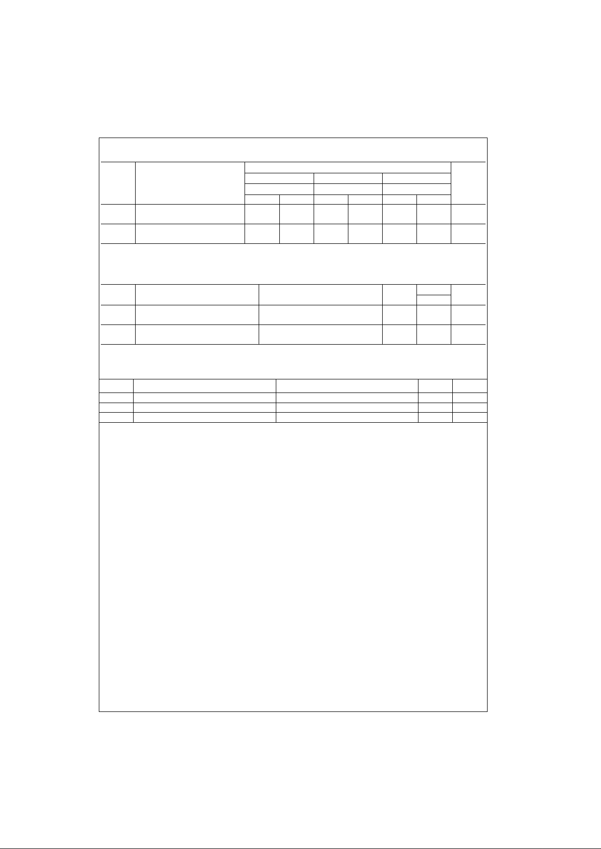
AC Electrical Characteristics
Note 4: Skew is def ined as the absol ut e v alue of the difference between the actu al propagation del ay f or any two separate outputs of the same device. The
specification applies t o any outputs switching in the same direction, ei th er HIGH-to-LOW (t
OSHL
) or LOW-to-HIGH (t
OSLH
).
Dynamic Switching Characteristics
Capacitance
Symbol Parameter
TA = −40°C to +85°C, RL = 500 Ω
Units
VCC = 3.3V ± 0.3V VCC = 2.7V VCC = 2.5V ± 0.2V
CL= 50 pF CL = 50 pF CL = 30 pF
Min Max Min Max Min Max
t
PZL
Propagation Delay Time 1.5 5.0 1.5 5.5 1.5 6.5
ns
t
PLZ
1.5 5.0 1.5 5.5 1.5 6.0
t
OSHL
Output to Output Skew 1.0
ns
t
OSLH
(Note 4) 1.0
Symbol Parameter Conditions
V
CC
(V)
TA = 25°C
Units
Typical
V
OLP
Quiet Output Dynamic Peak V
OL
CL = 50 pF, VIH = 3.3V, VIL = 0V 3.3 0.8
V
CL = 30 pF, VIH = 2.5V, VIL = 0V 2.5 0.6
V
OLV
Quiet Output Dynamic Valley V
OL
CL = 50 pF, VIH = 3.3V, VIL = 0V 3.3 −0.8
V
CL = 30 pF, VIH = 2.5V, VIL = 0V 2.5 −0.6
Symbol Parameter Conditions Typical Units
C
IN
Input Capacitance VCC = Open, VI = 0V or V
CC
7pF
C
OUT
Output Capacitance VCC = 3.3V, VI = 0V or V
CC
8pF
C
PD
Power Dissipation Capacitance VCC = 3.3V, VI = 0V or VCC, f = 10 MHz 25 pF
 Loading...