

Fairchild Semiconductor 74LCX32500 Datasheet
April 2001
Revised June 2002
74LCX32500
Low Voltage 36-Bit Universal Bus Transceivers
with 5V Tolerant Inputs and Outputs
74LCX32500 Low Voltage 36-Bit Universal Bus Transceivers with 5V Tolerant Inputs and Outputs
General Description
These 36-bit universal bus transceivers combine D-type
latches and D-type flip-flops to allow data flow in transparent, latched, and clocked modes.
Data flow in each dir ection is controlled by output-enable
(OEAB and OEBA
clock (CLKAB
The LCX32500 is desi gned for low vol tage (2.5V or 3.3V )
V
applications with the capability of interfacing to a 5V
CC
signal environment.
The LCX32500 is fabricated with an advanced CMOS tech-
nology to achieve high s peed operation while maintaining
CMOS low power.
), latch-enable (LEAB and LEBA), and
and CLKBA) inputs.
Features
■ 5V tolerant inputs and outputs
■ 2.3V–3.6V V
■ 6.0 ns t
■ Power down high impedance inputs and outputs
■ Supports live insertion/withdrawal (Note 1)
■
±24 mA output drive (V
■ Uses patented noise/EMI reductio n circuitr y
■ Latch-up performance exce eds 500 mA
■ ESD performance:
Human body model
Machine model
■ Packaged in plastic Fine-Pitch Ball Grid Array (FBGA)
Note 1: To ensure the high-impedance state during power up or down, OE
should be tied to V
value or the resis tor i s det erm ined by t he c urren t-s ourc ing c apab ility of the
driver.
specifications provided
CC
max (VCC = 3.3V), 20 µA ICC max
PD
> 200V
and OE tied to GND thro ugh a res istor : the minimu m
CC
Ordering Code:
Order Number Package Number Package Description
74LCX32500G
(Note 2)(Note 3)
Note 2: Ordering code “G” indicates Trays.
Note 3: Devices also available in Tape and Reel. Specify by appending th e s uffix let t er “X” to the ordering code.
BGA114A 114-Ball Fine-Pitch Ball Grid Array (FBGA), JEDEC MO-205, 5.5mm Wide
= 3.0V)
CC
> 2000V
© 2002 Fairchild Semiconductor Corporation DS500406 www.fairchildsemi.com
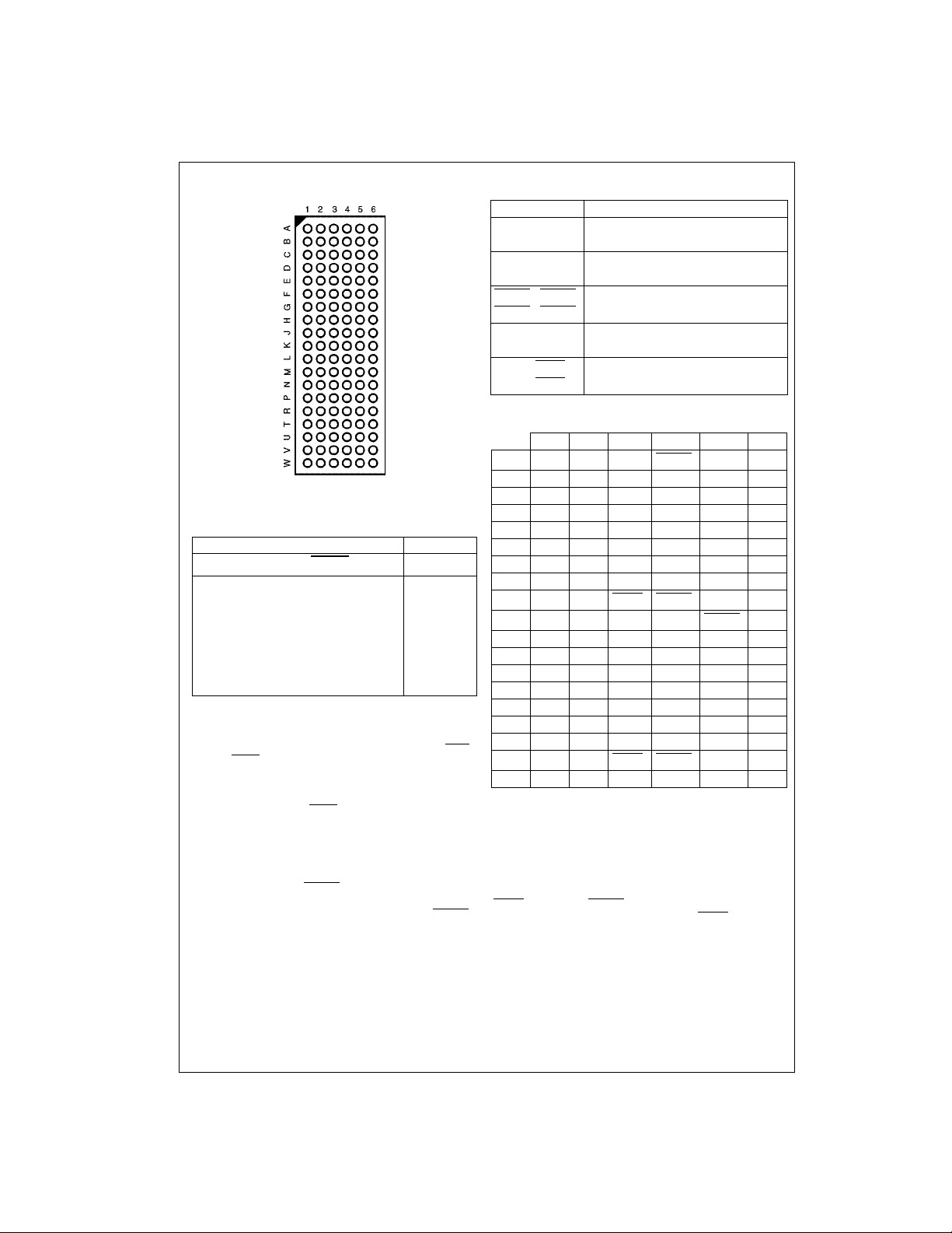
Connection Diagram
74LCX32500
(Top Thru View)
Truth Table (Note 4)
Inputs Output
OEAB
H = HIGH Voltage Level
L = LOW Voltage Level
X = Immaterial (HIGH or LOW, inputs may not float)
Z = High Impedance
Note 4: A-to-B data flow is shown: B-to-A flow is similar but uses OEBA
LEBA, and CLKBA
Note 5: Output level befor e the indicated steady-state input conditions
were established.
Note 6: Output level befor e the indicated steady-state input conditions
were established, provided that CLKAB
LEABnCLKABnA
n
n
LX XXZ
HH XL L
HH XHH
HL
HL
HL HXB
HL LXB
.
↓ LL
↓ HH
0
0
was LOW before LEAB went LOW.
B
n
(Note 5)
(Note 6)
Pin Descriptions
Pin Names Description
1A
- 1A
1
2A
- 2A
1
1B1 - 1B
2B
- 2B
1
18
18
18
18
Data Register A Inputs/3-STATE Outputs
Data Register B Inputs/3-STATE Outputs
CLKAB1, CLKBA1Clock Pulse Inputs
CLKAB
, CLKBA
2
2
LEAB1, LEBA1Latch Enable Inputs
, LEBA
LEAB
2
2
OEAB1, OEBA1Output Enable Inputs
, OEBA
OEAB
2
2
FBGA Pin Assignments
12 3 4 5 6
A 1A
B 1A41A3OEAB1GND 1B31B
C 1A61A5GND GND 1B51B
D 1A81A7V
E 1A101A9GND GND 1B91B
F 1A121A11GND GND 1B111B
G 1A141A13V
H 1A151A16GND GND 1B161B
J 1A171A18OEBA1CLKBA11B181B
K NC LEAB2LEBA1GND CLKAB2NC
L 2A
M 2A42A3GND GND 2B32B
N 2A62A5V
P 2A82A7GND GND 2B72B
R 2A102A9GND GND 2B92B
T 2A122A11V
U 2A142A13GND GND 2B132B
,
V 2A152A16OEBA2CLKBA22B162B
W 2A172A18LEBA2GND 2B182B
1A1LEAB1CLKAB11B11B
2
V
CC
CC
V
CC
CC
2A1OEAB2GND 2B12B
2
V
CC
CC
V
CC
CC
1B71B
1B131B
2B52B
2B112B
2
4
6
8
10
12
14
15
17
2
4
6
8
10
12
14
15
17
Functional Description
For A-to-B data flow, the LCX32500 ope rates in the transparent mode when L EAB is HIGH. When LEAB is LOW,
the A data is latched if CLKAB
logic level. If LEAB is LOW, the A bus data is stored in the
latch/flip-flop on the HIGH-to-LOW transition of CLKAB
Output-enable OEAB is active-HIGH. When OEAB is
www.fairchildsemi.com 2
is held at a HIGH or LOW
.
HIGH, the outputs are active. When OEAB is L OW, the outputs are in the high impedance state.
Data flow for B to A is similar to th at of A to B but uses
OEBA
, LEBA, and CLKBA. The output enables are com-
plementary (OEAB is active HIGH and OEBA
is active
LOW).
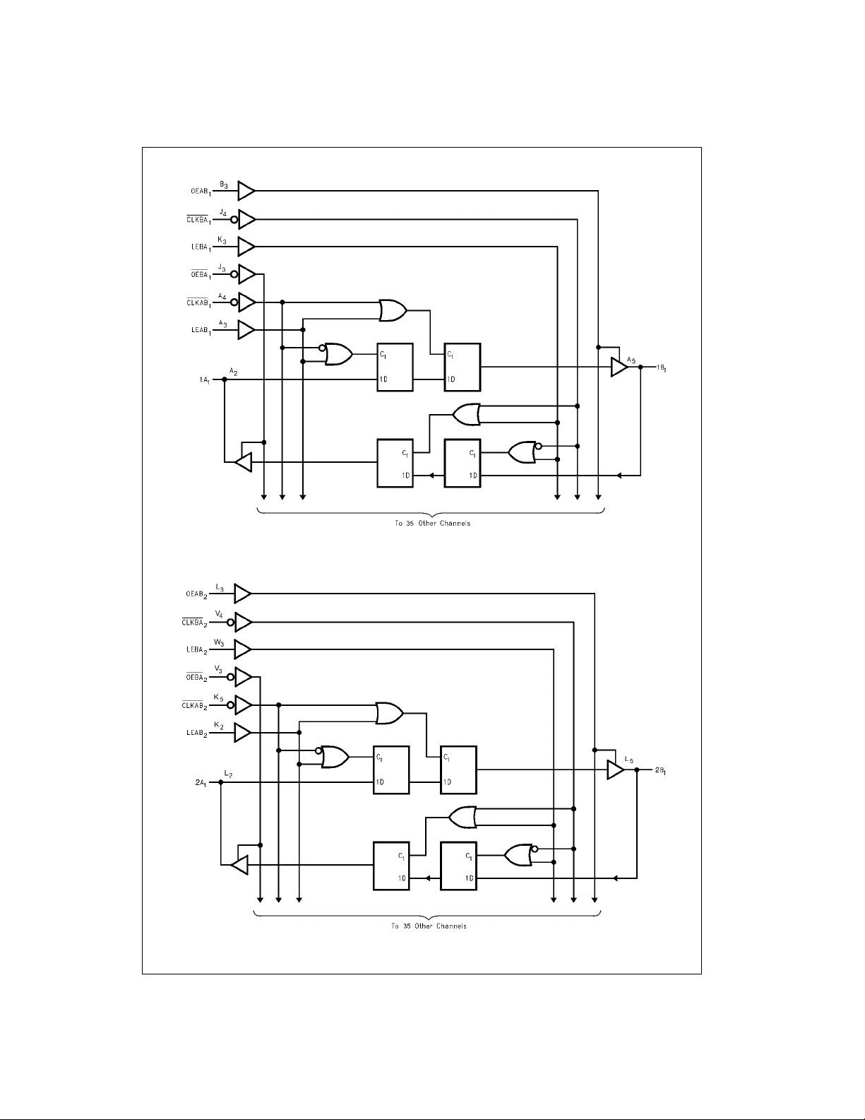
Logic Diagrams
74LCX32500
3 www.fairchildsemi.com
 Loading...