

Fairchild Semiconductor 74LCX32373 Datasheet
January 2001
Revised August 2001
74LCX32373
Low Voltage 32-Bit Transparent Latch
with 5V Tolerant Inputs and Outputs (Preliminary)
Preliminary
74LCX32373 Low Voltage 32-Bit Transparent Latch with 5V Tolerant Inputs and Outputs (Preliminary)
General Description
The LCX32373 contains thirty-two non-inverting latches
with 3-STATE outputs and is intended for bus oriented
applications. The device is byte controlled. The flip-flops
appear transparent to the data when the Latch Enable (LE)
is HIGH. When LE is LOW, the data that meets the setup
time is latched. Data appears o n the bus when th e Output
Enable (OE
a high impedance state.
The LCX32373 is desi gned for low vol tage (2.5V or 3.3V )
V
CC
environment.
The LCX32373 is fabricated with an advanced CMOS tech-
nology to achieve high s peed operation while maintaining
CMOS low power dissipation.
) is LOW. When OE is HIGH, the outputs are in
applications with capability of interfacing to a 5V signal
Features
■ 5V tolerant inputs and outputs
■ 2.3V–3.6V V
■ 5.4 ns t
■ Power down high impedance inputs and outputs
■ Supports live insertion/withdrawal (Note 1)
■
±24 mA output drive (V
■ Uses patented noise/EMI reductio n circuitr y
■ Latch-up performance exce eds 500 mA
■ ESD performance:
Human body model
Machine model
■ Packaged in plastic Fine-Pitch Ball Grid Array (FBGA)
(Preliminary)
Note 1: To ensure the high-impedance state during power up or down, OE
should be tied to VCC through a pull-up res istor: the m inimu m value or t he
resistor is determin ed by the current-sourc ing capability of the driver.
specifications provided
CC
max (VCC = 3.3V), 20 µA ICC max
PD
> 200V
Ordering Code:
Order Number Package Number Package Description
74LCX32373GX
(Note 2)
Note 2: BGA package available in Tape and Reel only.
BGA96A
(Preliminary)
96-Ball Fine-Pitch Ball Grid Array (FBGA), JEDEC MO-205, 5.5mm Wide
[TAPE and REEL]
Logic Symbol
= 3.0V)
CC
> 2000V
© 2001 Fairchild Semiconductor Corporation DS500547 www.fairchildsemi.com
Preliminary
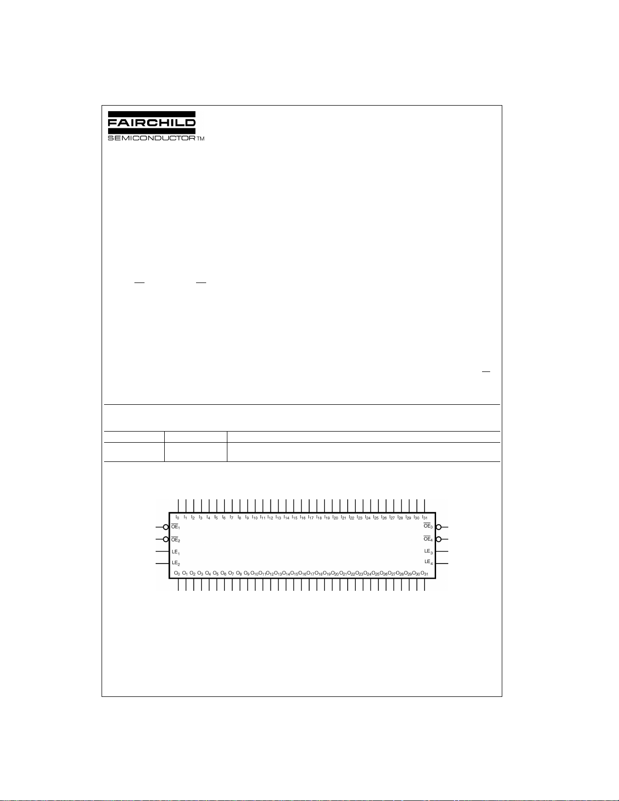
Connection Diagram
74LCX32373
(Top Thru View)
Pin Descriptions
Pin Names Description
OE
n
LE
n
I
- I
0
31
O
- O
0
31
Output Enable Input (Active LOW)
Latch Enable Input
FBGA Pin Assignments
123456
A O
B O
C O
D O
E O
F O
G O
H O
J O
K O
L O
M O
N O
P O
R O
T O
O0OE1LE
1
O2GND GND I
3
O4V
5
7
9
O10V
11
13O12
14O15
17O16
19O18
21O20VCCVCCI20I21
23O22
25O24
27O26VCCVCCI26I27
29O28
30O31
CCVCCI4
O6GND GND I
O8GND GND I
CCVCCI10I11
GND GND I
OE2LE2I
OE3LE3I
GND GND I
GND GND I
GND GND I
GND GND I
OE4LE4I
Inputs
Outputs
1I0
2
6
8
12I13
15I14
16I17
18I19
22I23
24I25
28I29
31I30
I
1
I
3
I
5
I
7
I
9
Functional Description
The LCX32373 contains thirty-two D-type latches with
3-STATE standard outputs. The dev ice is byte controlled
with each byte f unctioning identically, but independent of
the other. Control pins can be shorted together to obtain full
32-bit operation. The following description applies to each
byte. When the Latch E nable (LE
the I
enters the latches. In this condition the latches are
n
transparent, i.e. a latch ou tput will change s tate each time
www.fairchildsemi.com 2
) input is HIGH, data on
n
Truth Table
Inputs Outputs
LE
n
XH X Z
HL L L
HL H H
LL X O
H = HIGH Voltage Level
L = LOW Voltage Level
X = Immaterial
Z = High Impedance
= Previous O0 before HIGH-to-LOW transition of Lat ch Enable
O
0
its I input changes. When LE
information that was pr esent on the I inputs a set up time
preceding the HIGH-to-LOW transition of LE
3-STATE standard outputs are controlled by the Output
Enable (OE
puts are in the 2-state mode. When OE
dard outputs are in the high impedance mode but this does
not interfere with entering new data into the latches.
OE
n
) input. When OEn is LOW, the standard out-
n
I
n
is LOW, the latches store
n
is HIGH, the stan-
n
O
n
0
n
. The
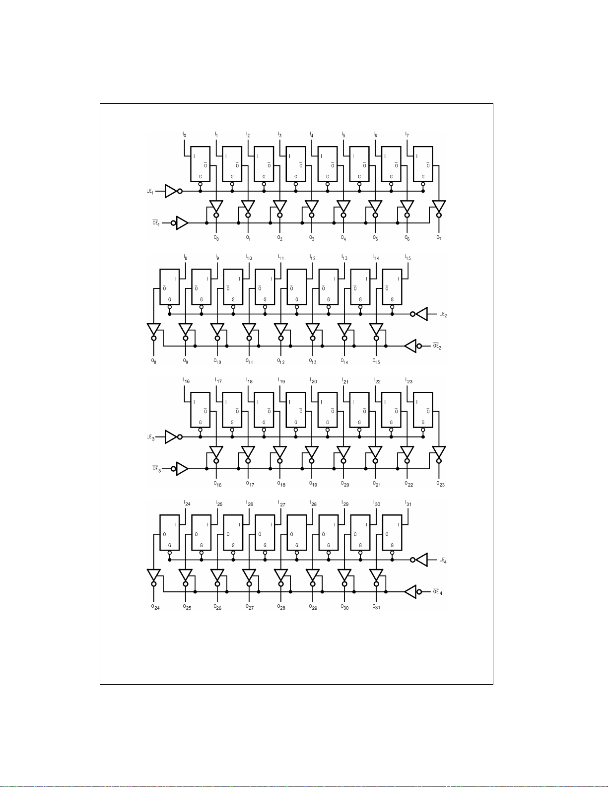
Logic Diagrams
Preliminary
74LCX32373
Please note that this diagram is provided only for the understanding of logic operations and should not be used to estimate propagation delays.
3 www.fairchildsemi.com
 Loading...