

Fairchild Semiconductor 74LCX32244 Datasheet
74LCX32244
Low Voltage 32-Bit Buffer/Line Driver
with 5V Tolerant Inputs and Outputs
74LCX32244 Low Voltage 32-Bit Buffer/Line Driver with 5V Tolerant Inputs and Outputs
April 2001
Revised June 2002
General Description
The LCX32244 contains thirty-two non-inverting buffers
with 3-STA TE outputs designed to be employed as a memory and address driver, clock driver, or bus oriented transmitter/receiver. The device is nibble controlled. Each nibble
has separate 3-STATE control inputs which can be shorted
together for full 32-bit operation.
The LCX32244 is desi gned for low vol tage (2.5V or 3.3V )
V
applications with capability of interfacing to a 5V signal
CC
environment.
The LCX32244 is fabricated with an advanced CMOS tech-
nology to achieve high s peed operation while maintaining
CMOS low power dissipation.
Features
■ 5V tolerant inputs and outputs
■ 2.3V–3.6V V
■ 4.5 ns t
■ Power down high impedance inputs and outputs
■ Supports live insertion/withdrawal (Note 1)
■
±24 mA output drive (V
■ Uses patented noise/EMI reductio n circuitr y
■ Latch-up performance exce eds 500 mA
■ ESD performance:
Human body model
Machine model
■ Packaged in plastic Fine-Pitch Ball Grid Array (FBGA)
Note 1: To ensure the high-impedance state during power up or down OE
should be tied to VCC through a pull-up res istor: the m inimu m value or t he
resistor is determin ed by the current-sourc ing capability of the driver.
specifications provided
CC
max (VCC = 3.0V), 20 µA ICC max
PD
> 200V
Ordering Code:
Order Number Package Number Package Description
74LCX32244G
(Note 2)(Note 3)
Note 2: Ordering code “G” indicates Trays.
Note 3: Devices also available in Tape and Reel. Specify by appending th e s uffix let t er “X” to the ordering code.
BGA96A 96-Ball Fine-Pitch Ball Grid Array (FBGA), JEDEC MO-205, 5.5mm Wide
Logic Symbol
= 3.0V)
CC
> 2000V
© 2002 Fairchild Semiconductor Corporation DS500426 www.fairchildsemi.com

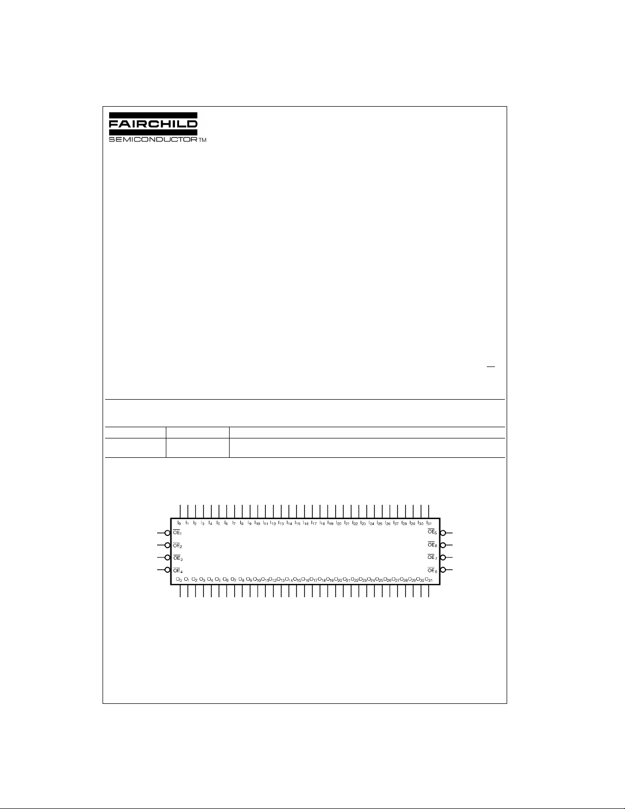
Connection Diagram
74LCX32244
(Top Thru View)
Functional Description
The LCX32244 contains thirty-two non-inverting buffers
with 3-STATE standard outputs. The device is nibble
(4-bits) controlled with each nibble functioning identically,
but independent of the other. The control pins can be
shorted together to obtain full 32-bit operation. The
3-STATE outputs are controlled by an Output Enable (OE
input for each nibble. When OE
2-state mode. When OE
high impedance mode, but this does not interfere with
entering new data into the inputs.
is LOW, the outputs are in
n
is HIGH, the outputs are in th e
n
Pin Descriptions
Pin Names Description
OE
I
0–I31
O
0–O31
n
Output Enable Input (Active LOW)
Inputs
Outputs
FBGA Pin Assignments
123456
A O
O0OE1OE2I
1
B O3O2GND GND I
C O5O4V
D O7O6GND GND I
E O
F 0
O8GND GND I
9
O10V
11
G O13O12GND GND I
H O14O15OE4OE3I
J O
17O16
K O
19018
L O21O20V
M O
23O22
N O25O24GND GND I
P O27O26V
R O29O28GND GND I
)
n
T O30O31OE8OE7I
Truth Table
Inputs Outputs
OE
n
LL L
LH H
HX Z
H = HIGH Voltage Level
L = LOW Voltage Level
X = Immaterial (HIGH or LOW, inputs may not float)
Z = High Impedance
I
n
0
2
CCVCCI4
6
8
CCVCCI10I11
12I13
15I14
OE5OE6I
GND GND I
CCVCCI20I21
GND GND I
CCVCCI26I27
16I17
18I19
22I23
24I25
28I29
31I30
O
n
I
1
I
3
I
5
I
7
I
9
Logic Diagrams
www.fairchildsemi.com 2
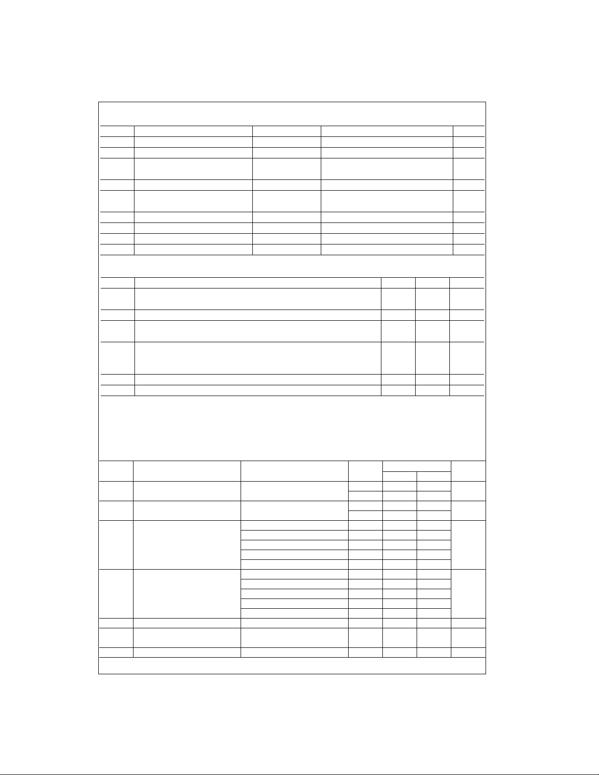
Absolute Maximum Ratings(Note 4)
Symbol Parameter Value Conditions Units
V
V
V
I
IK
I
OK
I
O
I
CC
I
GND
T
CC
I
O
STG
Supply Voltage −0.5 to +7.0 V
DC Input Voltage −0.5 to +7.0 V
DC Output Voltage −0.5 to +7.0 Output in 3-STATE
−0.5 to V
+ 0.5 Output in HIGH or LOW St ate (Note 5)
CC
DC Input Diode Current −50 VI < GND mA
DC Output Diode Current −50 VO < GND
+50 V
O
> V
CC
mA
DC Output Source/Sink Current ±50 mA
DC Supply Current per Supply Pin ±100 mA
DC Ground Current per Ground Pin ±100 mA
Storage Temperature −65 to +150 °C
Recommended Operating Conditions (Note 6)
Symbol Parameter Min Max Units
V
CC
V
I
V
O
I
OH/IOL
T
A
∆t/∆V Input Edge Rate, V
Note 4: The Absolute Maximum Ratings are those values beyond which the safety of the device cannot be guaranteed. The device should not be operated
at these limits. The parametric values defined in the Electrical Characteristics tables are not guaranteed at the Absolute Maximum Ratings. The “Recom-
mended Operating Conditions” table will define the condition s fo r ac t ual device operation.
Note 5: I
Note 6: Unused inputs must be held HIGH or LOW. They may not flo at .
Supply Voltage Operating 2.0 3.6
Data Retention 1.5 3.6
V
Input Voltage 05.5V
Output Voltage HIGH or LOW State 0 V
3-STATE 0 5.5
CC
V
Output Current VCC = 3.0V − 3.6V ±24
= 2.7V − 3.0V ±12
CC
V
= 2.3V − 2.7V ±8
CC
mAV
Free-Air Operating T emperature −40 85 °C
= 0.8V–2.0V, VCC = 3.0V 0 10 ns/V
IN
Absolute Maximum Rating must be observed.
O
74LCX32244
V
DC Electrical Characteristics
Symbol Parameter Conditions
V
V
V
V
I
I
I
IH
IL
OH
OL
I
OZ
OFF
HIGH Level Input Voltage 2.3 − 2.7 1.7
LOW Level Input Voltage 2.3 − 2.7 0.7
HIGH Level Output Voltage IOH = −100 µA2.3 − 3.6 VCC − 0.2
LOW Level Output Voltage IOL = 100 µA2.3 − 3.6 0.2
Input Leakage Current 0 ≤ VI ≤ 5.5V 2.3 − 3.6 ±5.0 µA
3-STATE Output Leakage 0 ≤ VO ≤ 5.5V
Power-Off Leakage Current VI or VO = 5.5V 0 10 µA
IOH = −8 mA 2.3 1.8
IOH = −12 mA 2.7 2.2
IOH = −18 mA 3.0 2.4
IOH = −24 mA 3.0 2.2
IOL = 8 mA 2.3 0.6
IOL = 12 mA 2.7 0.4
IOL = 16 mA 3.0 0.4
IOL = 24 mA 3.0 0.55
VI = VIH or V
IL
3 www.fairchildsemi.com
V
TA = −40°C to +85°C
CC
(V) Min Max
2.7 − 3.6 2.0
2.7 − 3.6 0.8
2.3 − 3.6 ±5.0 µA
Units
V
V
V
V
 Loading...