

Fairchild Semiconductor 74LCX27 Datasheet
74LCX27
Low Voltage Triple 3-Input NOR Gate
with 5V Tolerant Inputs
74LCX27 Low Voltage Triple 3-Input NOR Gate with 5V Tolerant Inputs
February 2001
Revised February 2001
General Description
The LCX27 contains three 3-input NOR g ates. The inputs
tolerate voltages up to 7V al lowing the in terface of 5 V systems to 3V systems.
The 74LCX27 is fabrica ted with advanced C MOS technology to achieve high speed operation while maintaining
CMOS low power dissipation.
Features
■ 5V tolerant inputs
■ 2.3V–3.6V V
■ 4.9 ns t
■ Power down high impedance inputs and outputs
■
±24 mA output drive (V
■ Implements patented noise/EMI reduction circuitry
■ Latch-up performance exce eds 500 mA
■ ESD performance:
Human body model
Machine model
specifications provided
CC
max (V
PD
CC
> 200V
= 3.3V), 10 µA I
= 3.0V)
CC
> 2000V
max
CC
Ordering Code:
Order Numbe r Package Numb er Package Description
74LCX27M M14A 14-Lead Small Outline Integrated Circuit (SOIC), JEDEC MS-012, 0.150 Narrow
74LCX27SJ M14D 14-Lead Small Outline Package (SOP), EIAJ TYPE II, 5.3mm Wide
74LCX27MTC MTC14 14-Lead Thin Shrink Small Outline Package (TSSOP), JEDEC MO-153, 4.4mm Wide
Devices also availab l e in Tape and Reel. Specify by appending th e s uffix let t er “X” to the ordering code.
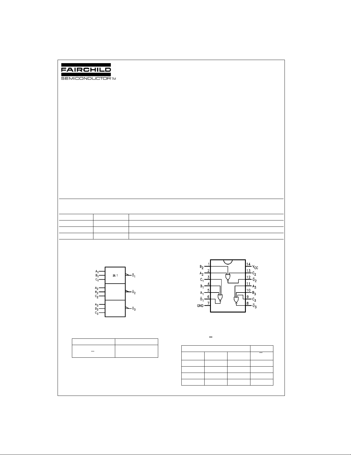
Logic Symbol
IEEE/IEC
Connection Diagram
Pin Descriptions Truth Table
Pin Names Descriptio n
, Bn, C
A
n
n
O
n
© 2001 Fairchild Semiconductor Corporation DS500454 www.fairchildsemi.com
Inputs
Outputs
A
HXXL
XHXL
XXHL
LLLH
H = HIGH Voltage Level L = LOW Voltage Level X = Immaterial
On = An + Bn + C
Inputs Output
n
B
n
n
C
n
O
n
Absolute Maximum Ratings(Note 1)
Symbol Parameter Value Conditions Units
74LCX27
V
V
V
I
IK
I
OK
I
O
I
CC
I
GND
T
CC
I
O
STG
Supply Voltage −0.5 to +7.0 V
DC Input Voltage −0.5 to +7.0 V
DC Output Voltage −0.5 to VCC + 0.5 Output in HIGH or LOW State (Note 2) V
DC Input Diode Current −50 VI < GND mA
DC Output Diode Current −50 VO < GND
+50 V
O
> V
CC
DC Output Source/Sink Current ±50 mA
DC Supply Current per Supply Pin ±100 mA
DC Ground Current per Ground Pin ±100 mA
Storage Temperature −65 to +150 °C
Recommended Operating Conditions (Note 3)
Symbol Parameter Min Max Units
V
V
V
I
OH/IOL
T
∆t/∆V Input Edge Rate, V
Note 1: The Absolute Maximum Ratings are those values beyond which the safety of the device cannot be guaranteed. The device should not be operated
at these limits. The parametric values defined in the Electrical Characteristics tables are not guaranteed at the Absolute Maximum Ratings. The “Recom-
mended Operat ing Conditions” table w ill define the condition s fo r ac t ual device operation.
Note 2: I
Note 3: Unused inputs must be held HIGH or LOW. They may not float.
Supply Voltage Operating 2.0 3.6
CC
Input Voltage 05.5V
I
Output Voltage HIGH or LOW State 0 V
O
Output Current VCC = 3.0V − 3.6V ±24
Free-Air Operating Temperature −40 85 °C
A
Absolute Maximum Rating must be observed.
O
Data Retention 1.5 3.6
CC
= 2.7V - 3.0V ±12
CC
= 2.3V - 2.7V ±8
V
CC
= 0.8V–2.0V, VCC = 3.0V 0 10 ns/V
IN
mA
V
V
mAV
DC Electrical Characteristics
Symbol Parameter Conditions
V
IH
V
IL
V
OH
V
OL
I
I
I
OFF
I
CC
∆I
www.fairchildsemi.com 2
HIGH Level Input Voltage 2.3 − 2.7 1.7
LOW Level Input Voltage 2.3 − 2.7 0.7
HIGH Level Output Voltage IOH = −100 µA2.3 − 3.6 VCC − 0.2
IOH = −8 mA 2.3 1.8
IOH = −12 mA 2.7 2.2
IOH = −18 mA 3.0 2.4
LOW Level Output Voltage IOL = 100 µA2.3 − 3.6 0.2
Input Leakage Current 0 ≤ VI ≤ 5.5V 2.3 − 3.6 ±5.0 µA
Power-Off Leakage Current VI or VO = 5.5V 0 10 µA
Quiescent Supply Current VI = VCC or GND 2.3 − 3.6 10
Increase in ICC per Input VIH = VCC −0.6V 2.3 − 3.6 500 µA
CC
IOH = −24 mA 3.0 2.2
IOL = 8mA 2.3 0.6
IOL = 12 mA 2.7 0.4
IOL = 16 mA 3.0 0.4
IOL = 24 mA 3.0 0.55
3.6V ≤ VI ≤ 5.5V 2.3 − 3.6 ±10
V
CC
(V) Min Max
2.7 − 3.6 2.0
2.7 − 3.6 0.8
TA = −40°C to +85°C
Units
V
V
V
V
µA
AC Electrical Characteristics
= −40°C to +85°CF, RL = 500Ω
T
A
Symbol Parameter
V
= 3.3V ± 0.3V VCC = 2.7V VCC = 2.5V ± 0.2V
CC
= 50pF CL = 50pF CL = 30pF
C
L
Min Max Min Max Min Max
t
PHL
t
PLH
t
OSHL
t
OSLH
Note 4: Skew is defined as t he absolute value of the difference between the actu al propagation delay for any two s eparate outputs of t he same device. T h e
specification applies t o any outputs switchi ng in the same direction, either HIGH-to-LOW (t
Propagation Delay 1.5 4.9 1.5 5.8 1.5 5.9
1.5 4 .9 1.5 5.8 1.5 5.9
Output to Output Skew (Note 4) 1.0
1.0
) or LOW-to-HIGH (t
OSHL
OSLH
).
Dynamic Switching Characteristics
Symbol Parameter Conditions
V
OLP
Quiet Output Dynamic Peak V
OL
CL = 50 pF, VIH = 3.3V, VIL = 0V 3.3 0 .8
CL = 30 pF, VIH = 2.5V, VIL = 0V 2.5 0 .6
V
OLV
Quiet Output Dynamic Valley V
OL
CL = 50 pF, VIH = 3.3V, VIL = 0V 3.3 −0.8
= 30 pF, VIH = 2.5V, VIL = 0V 2.5 −0.6
C
L
V
(V) Typical
CCTA
= 25°C
Capacitance
Symbol Parameter Conditions Typical Units
C
IN
C
OUT
C
PD
Input Capacitance VCC = Open, VI = 0V or V
Output Capacitance VCC = 3.3V, VI = 0V or V
CC
CC
7pF
8pF
Power Dissipation Capacitance VCC = 3.3V, VI = 0V or VCC, f = 10 MHz 25 pF
74LCX27
Units
ns
ns
Unit
V
V
3 www.fairchildsemi.com
 Loading...