

Fairchild Semiconductor 74LCX257SJX, 74LCX257SJ, 74LCX257MX, 74LCX257MTCX, 74LCX257MTC Datasheet
...
© 2000 Fairchild Semiconductor Corporation DS012466 www.fairchildsemi.com
May 1995
Revised September 2000
74LCX257 Low Voltage Quad 2-Input Multiplexer with 5V Tolerant Inputs and Outputs
74LCX257
Low Voltage Quad 2-Input Multiplexer
with 5V Tolerant Inputs and Outputs
General Description
The LCX257 is a quad 2 -input multiplexer with 3-STATE
outputs. Four bits of data from two sources can be selected
using a Common Data Select input. The four outputs
present the selected da ta in true (non i nverted) form. The
outputs may be switched to a high impedance state by
placing a logic HIGH on the commo n Output Enable (OE
)
input, allowing the outpu ts to i nt erf ace d irectly with bus-oriented systems.
The 74LCX257 is fabricated with advanced CMOS technology to achieve high speed operation while maintaining
CMOS low power dissipation.
Features
■ 5V tolerant inputs and outputs
■ 2.3V–3.6V V
CC
specifications provided
■ 6.0 ns t
PD
max (VCC = 3.3V, In → Zn), 10 µA ICC max
■ Power down high impedance inputs and outputs
■ Supports live insertion/withdrawal (Note 1)
■ Implements patented noise/EMI reduction circuitry
■ Latch-up performance exce eds 500 mA
■ ESD performance:
Human body model
> 2000V
Machine model
> 200V
Note 1: To ensure the high-impedance state during power up or down, OE
should be tied to VCC through a pull-up res istor: the m inimu m value or t he
resistor is determin ed by the current-sourcin g c apability of the driver.
Ordering Code:
Devices also availab le in Tape and Reel. Specify by appending th e s uffix let t er “X” to the ordering code.
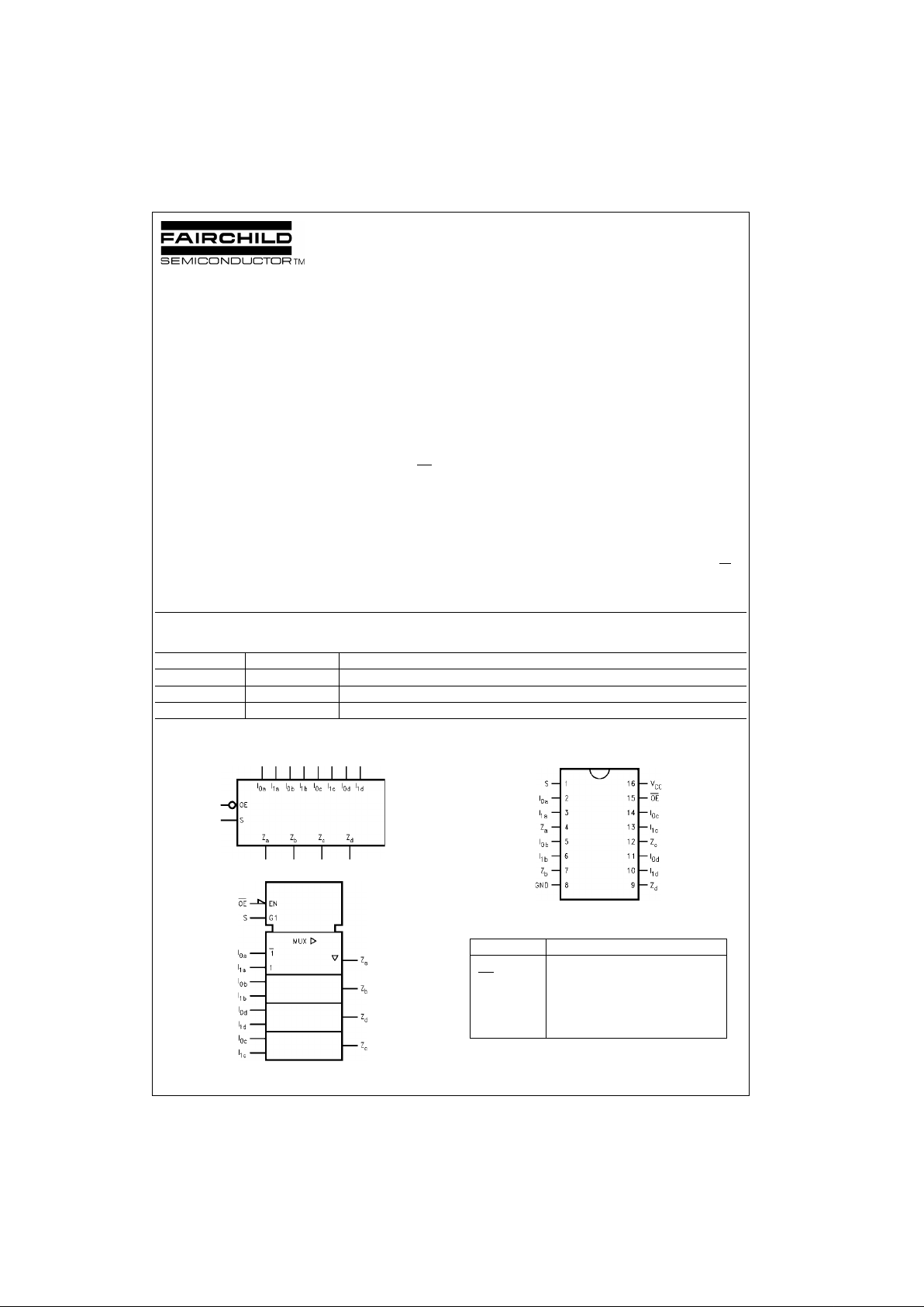
Logic Symbols
IEEE/IEC
Connection Diagram
Pin Descriptions
Order Number Package Number Package Description
74LCX257M M16A 16-Lead Small Outline Integrated Circuit (SOIC), JEDEC MS-012, 0.150 Narrow
74LCX257SJ M16D 16-Lead Small Outline Package (SOP), EIAJ TYPE II, 5.3mm Wide
74LCX257MTC MTC16 16-Lead Thin Shrink Small Outline Package (TSSOP), JEDEC MO-153, 4.4mm Wide
Pin Names Description
S Common Data Select Input
OE 3-STATE Output Enable Input
I
0a–I0d
Data Inputs from Source 0
I
1a–I1d
Data Inputs from Source 1
Z
a–Zd
3-STATE Multiplexer Outputs
www.fairchildsemi.com 2
74LCX257
Functional Description
The LCX257 is a quad 2-input multiplexer with 3-STATE
outputs. It selects fo ur bits of dat a from two so urces u nder
control of a Common Data Selec t input. When the Select
input is LOW, the I
0x
inputs are selected and when Select
is HIGH, the I
1x
inputs are selected. The data on the
selected inputs appears at the outputs in true (non
inverted) form. The de vice is the l ogic imple mentation o f a
4-pole, 2-position switch w he re the position of the switch is
determined by the logic l evels sup plied to the Select i nput.
The logic equations for the outputs are shown below:
Z
a
= OE • (11a • S + I0a • S)
Z
b
= OE • (11b • S + I0b • S)
Z
c
= OE • (11c • S + I0c • S)
Z
d
= OE • (11d • S + I0d • S)
When the Output Enab le (OE
) is HIGH, the outputs are
forced to a high impedance state. If the outp uts are tied
together, all but one device m ust be i n the hig h im pe dance
state to avoid h igh currents that wou ld exceed the maximum ratings. Designe rs should ensure th e Output Enable
signals to 3-STATE devices whose outputs are tied
together are designed so there is no overlap.
Tr uth Table
H = HIGH Voltage Level
L = LOW Voltage Level
X = Immaterial
Z = High Impedance
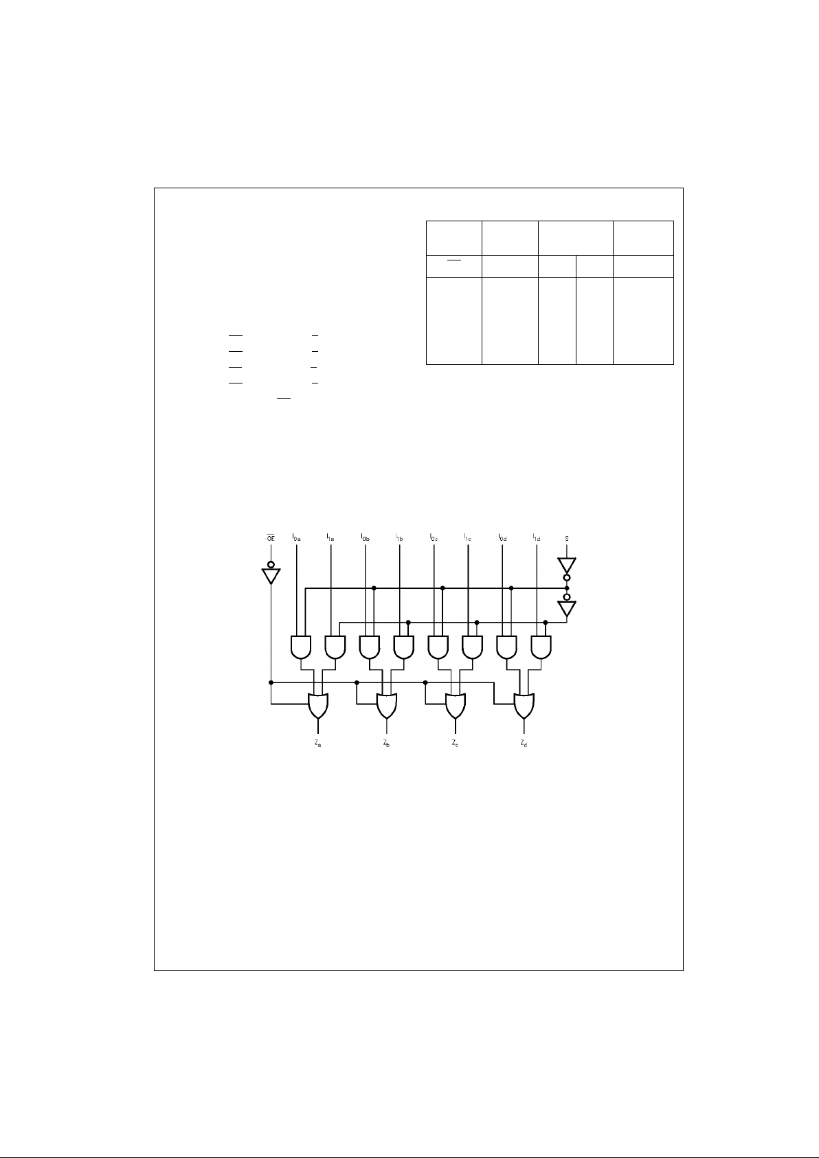
Logic Diagram
Please note that this diagram is provided only for the understanding of logic operations and should not be used to estimate propagation delays.
Output Select Data Outputs
Enable Input Inputs
OE
SI0I
1
Z
HXXXZ
LHXLL
LHXHH
LLLXL
LLHXH
3 www.fairchildsemi.com
74LCX257
Absolute Maximum Ratings(Note 1)
Recommended Operating Conditions (Note 4)
Note 2: The Absolute Maximum Ratings are those values beyond which the safety of the device cannot be guaranteed. The device should not be operated
at these limits. The parametric values defined in the Electrical Characteristics tables are not guaranteed at the Absolute Maximum Ratings. The “Recom-
mended Operating Conditions” table will define the conditions fo r ac t ual device operation.
Note 3: I
O
Absolute Maximum rating must be observed.
Note 4: Unused Inputs must be held HIGH or LOW. They may not float.
DC Electrical Characteristics
Symbol Parameter Value Conditions Units
V
CC
Supply Voltage −0.5 to +7.0 V
V
I
DC Input Voltage −0.5 to +7.0 V
V
O
DC Output Voltage −0.5 to +7.0 Output in 3-STATE
V
−0.5 to V
CC
+ 0.5 Output in HIGH or LOW State (Note 2)
I
IK
DC Input Diode Current −50 VI < GND mA
I
OK
DC Output Diode Current −50 VO < GND
mA
+50 V
O
> V
CC
I
O
DC Output Source/Sink Current ±50 mA
I
CC
DC Supply Current per Supply Pin ±100 mA
I
GND
DC Ground Current per Ground Pin ±100 mA
T
STG
Storage Temperature −65 to +150 °C
Symbol Parameter Min Max Units
V
CC
Supply Voltage Operating 2.0 3.6
V
Data Retention 1.5 3.6
V
I
Input Voltage 05.5V
V
O
Output Voltage HIGH or LOW State 0 V
CC
V
3-STATE 0 5.5
I
OH/IOL
Output Current VCC = 3.0V − 3.6V ±24
V
CC
= 2.7V − 3.0V ±12 mA
V
CC
= 2.3V − 2.7V ±8
T
A
Free-Air Operating Temperature −40 85 °C
∆t/∆V Input Edge Rate, V
IN
= 0.8V–2.0V, VCC = 3.0V 0 10 ns/V
Symbol Parameter Conditions
V
CC
TA = −40°C to +85°C
Units
(V) Min Max
V
IH
HIGH Level Input Voltage 2.3 − 2.7 1.7
V
2.7 − 3.6 2.0
V
IL
LOW Level Input Voltage 2.3 − 2.7 0.7
V
2.7 − 3.6 0.8
V
OH
HIGH Level Output Voltage IOH = −100 µA2.3 − 3.6 VCC − 0.2
V
IOH = −8 mA 2.3 1.8
IOH = −12 mA 2.7 2.2
IOH = −18 mA 3.0 2.4
IOH = −24 mA 3.0 2.2
V
OL
LOW Level Output Voltage IOL = 100 µA2.3 − 3.6 0.2
V
IOL = 8 mA 2.3 0.6
IOL = 12 mA 2.7 0.4
IOL = 16 mA 3.0 0.4
IOL = 24 mA 3.0 0.55
I
I
Input Leakage Current 0 ≤ VI ≤ 5.5V 2.3 − 3.6 ±5.0 µA
I
OZ
3-STATE Output Leakage 0 ≤ VO ≤ 5.5V
2.3 − 3.6 ±5.0 µA
VI = VIH or V
IL
I
OFF
Power-Off Leakage Current VI or VO = 5.5V 0 10 µA
 Loading...