

Fairchild Semiconductor 74LCX240WMX, 74LCX240WM, 74LCX240SJX, 74LCX240SJ, 74LCX240MTCX Datasheet
...
February 1994
Revised April 1999
74LCX240 Low Voltage Octal Buffer/Line Driver with 5V Tolerant Inputs and Outputs
© 1999 Fairchild Semiconductor Corporation DS011993.prf www.fairchildsemi.com
74LCX240
Low Voltage Octal Buffer/Line Driver with
5V Tolerant Inputs and Outputs
General Description
The LCX240 is an inverting octal buffer and line driver
designed to be employed as a memory address driver,
clock driver and bus oriented tra nsmitter or receiver. The
device is designed for low voltage (2.5V or 3.3V) V
CC
appli-
cations with capability of i n ter facin g to a 5 V sign al environment.
The LCX240 is fabrica ted with an advanced CMOS technology to achieve high spee d operation while mai ntaining
CMOS low power dissipation.
Features
■ 5V tolerant inputs and outputs
■ 2.3V–3.6V V
CC
specifications provided
■ 6.5 ns t
PD
max (VCC = 3.3V), 10 µA ICC max
■ Power-down high impedance inputs and outputs
■ Supports live insertion/withdrawal (Note 1)
■ ±24 mA output drive (V
CC
= 3.0V)
■ Implements patented noise/EMI reduction circuitry
■ Latch-up performance exceeds 500 mA
■ ESD performance:
Human body model > 2000V
Machine model > 200V
Note 1: To ensure the high-impedan c e state during power up or down, OE
should be tied to VCC through a pull-up res istor: the m inimu m value or t he
resistor is determin ed by the current-sourcing capability of the dr iv er.
Ordering Code:
Devices also availab le in Tape and Reel. Specify by appending th e s uffix let t er “X” to the ordering code.
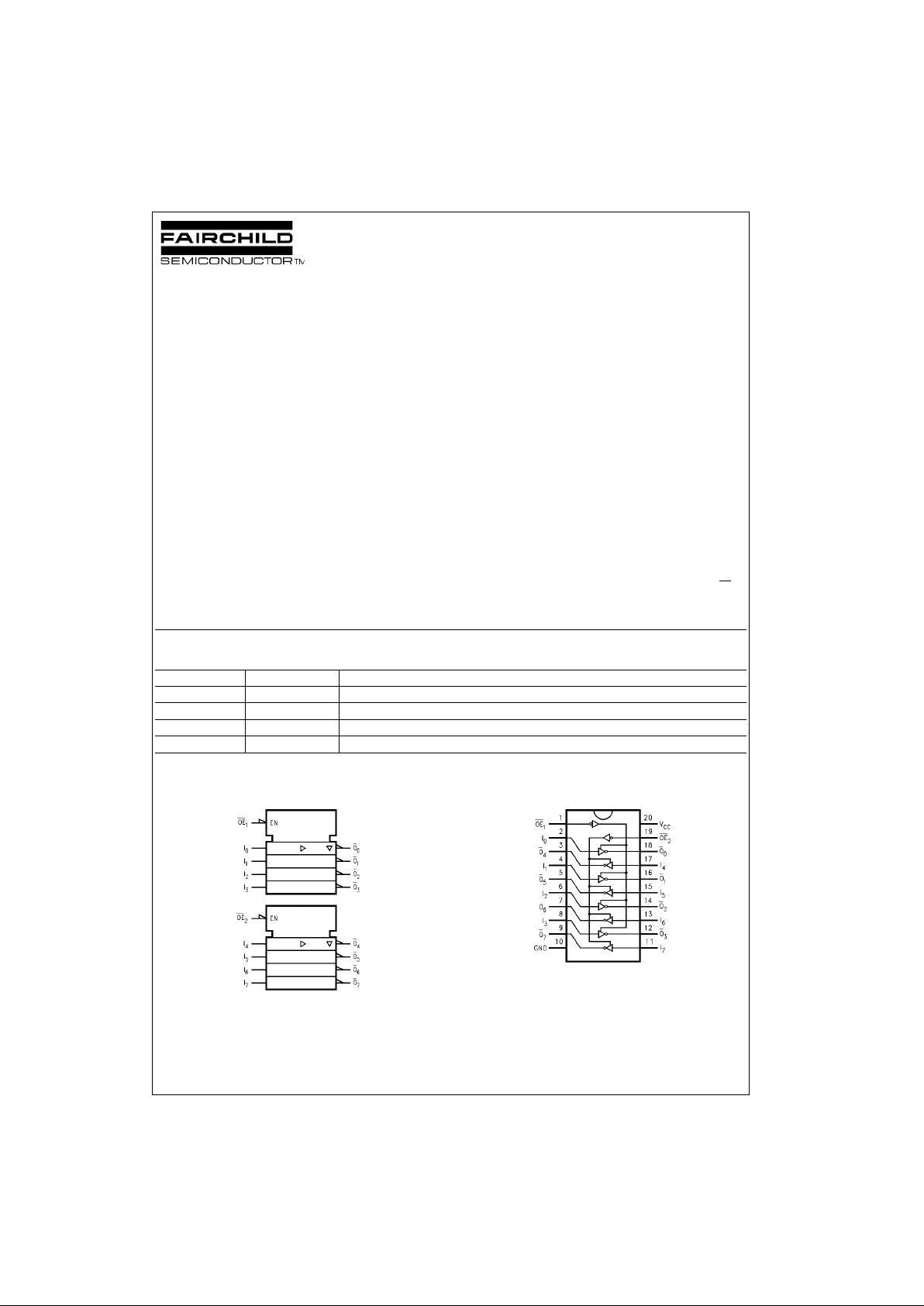
Logic Diagram Connection Diagram
Order Number Package Number Package Description
74LCX240WM M20B 20-Lead Small Outline Integrated Circuit (SOIC), JEDEC MS-013, 0.300” Wide
74LCX240SJ M20D 20-Lead Small Outline Package (SOP), EIAJ TYPE II, 5.3mm Wide
74LCX240MSA MSA20 20-Lead Shrink Small Outline Package (SSOP), EIAJ TYPE II, 5.3mm Wide
74LCX240MTC MTC20 20-Lead Thin Shrink Small Outline Package (TSSOP), JEDEC MO-153, 4.4mm Wide
www.fairchildsemi.com 2
74LCX240
Pin Descriptions
Truth Tables
H = HIGH Voltage Level
L = LOW Voltage Level
X = Immaterial
Z = High Impedance
Pin Names Description
OE
1
, OE
2
3-STATE Output Enable Inputs
I
0–I7
Inputs
O
0–O7
Outputs
Inputs Outputs
(Pins 12, 14, 16, 18)
OE
1
I
n
LL H
LH L
HX Z
Inputs Outputs
OE
2
I
n
(Pins 3, 5, 7, 9)
LL H
LH L
HX Z
3 www.fairchildsemi.com
74LCX240
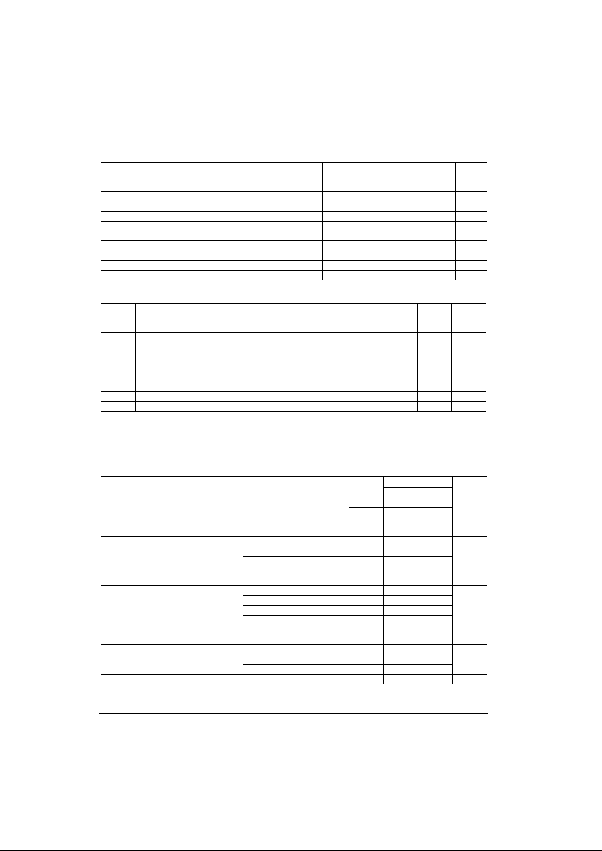
Absolute Maximum Ratings(Note 2)
Recommended Operating Conditions (Note 4)
Note 2: The Absolute Maximum Ratings are those values beyond which the safety of the device cannot be guaranteed. The device should not be operated
at these limits. The parametric values defined in the Electrical Characteristics tables are not guaranteed at the Absolute Maximum Ratings. The “Recommended Operating C onditions” table will def ine the conditions for actual device operation.
Note 3: I
O
Absolute Maximum Rating must be observed.
Note 4: Unused inputs must be held HIGH or LOW. They may not float.
DC Electrical Characteristics
Note 5: Outputs disab led or 3-STATE only.
Symbol Parameter Value Conditions Units
V
CC
Supply Voltage −0.5 to +7.0 V
V
I
DC Input Voltage −0.5 to +7.0 V
V
O
DC Output Voltage −0.5 to +7.0 Output in 3-STATE V
−0.5 to V
CC
+ 0.5 Output in HIGH or LOW State (Note 3) V
I
IK
DC Input Diode Current −50 VI < GND mA
I
OK
DC Output Diode Current −50 VO < GND
mA
+50 V
O
> V
CC
I
O
DC Output Source/Sink Current ±50 mA
I
CC
DC Supply Current per Supply Pin ±100 mA
I
GND
DC Ground Current per Ground Pin ±100 mA
T
STG
Storage Temperature −65 to +150 °C
Symbol Parameter Min Max Units
V
CC
Supply Voltage Operating 2.0 3.6
V
Data Retention 1.5 3.6
V
I
Input Voltage 05.5V
V
O
Output Voltage HIGH or LOW State 0 V
CC
V
3-STATE 0 5.5
IOH/I
OL
Output Current VCC = 3.0V − 3.6V ±24
mAVCC = 2.7V − 3.0V ±12
VCC = 2.3V − 2.7V ±8
T
A
Free-Air Operating Temperature −40 85 °C
∆t/∆V Input Edge Rate, V
IN
= 0.8V–2.0V, VCC = 3.0V 0 10 ns/V
Symbol Parameter Conditions
V
CC
TA = −40°C to +85°C
Units
(V) Min Max
V
IH
HIGH Level Input Voltage 2.3 − 2.7 1.7
V
2.7 − 3.6 2.0
V
IL
LOW Level Input Voltage 2.3 − 2.7 0.7
V
2.7 − 3.6 0.8
V
OH
HIGH Level Output Voltage IOH = −100µA2.3 − 3.6 VCC - 0.2
V
IOH = -8 mA 2.3 1.8
IOH = −12 mA 2.7 2.2
IOH = −18 mA 3.0 2.4
IOH = −24 mA 3.0 2.2
V
OL
LOW Level Output Voltage IOL = 100µA2.3 − 3.6 0.2
IOL = 8mA 2.3 0.6
IOL = 12 mA 2.7 0.4 V
IOL = 16 mA 3.0 0.4
IOL = 24 mA 3.0 0.55
I
I
Input Leakage Current 0 ≤ VI ≤ 5.5V 2.3 − 3.6 ±5.0 µA
I
OFF
Power-Off Leakage Current VI or VO = 5.5V 10 µA
I
CC
Quiescent Supply Current VI = VCC or GND 2.3 − 3.6 10
µA
3.6V ≤ VI, VO ≤ 5.5V (Note 5) 2.3 − 3.6 ±10
∆I
CC
Increase in I
CC
per Input VIH = VCC = 0.6V 2.3 − 3.6 500 µA
 Loading...