

Fairchild Semiconductor 74LCX2244WMX, 74LCX2244SJX, 74LCX2244SJ, 74LCX2244MTCX, 74LCX2244MTC Datasheet
...
© 1999 Fairchild Semiconductor Corporation DS012569 www.fairchildsemi.com
October 1995
Revised June 1999
74LCX2244 Low Voltage Buffer/Line Driver with 5V Tolerant Inputs and Outputs with 26Ω Series Resistors in the
Outputs
74LCX2244
Low Voltage Buffer/Line Driver with 5V Tolerant Inputs
and Outputs with 26Ω Series Resistors in the Outputs
General Description
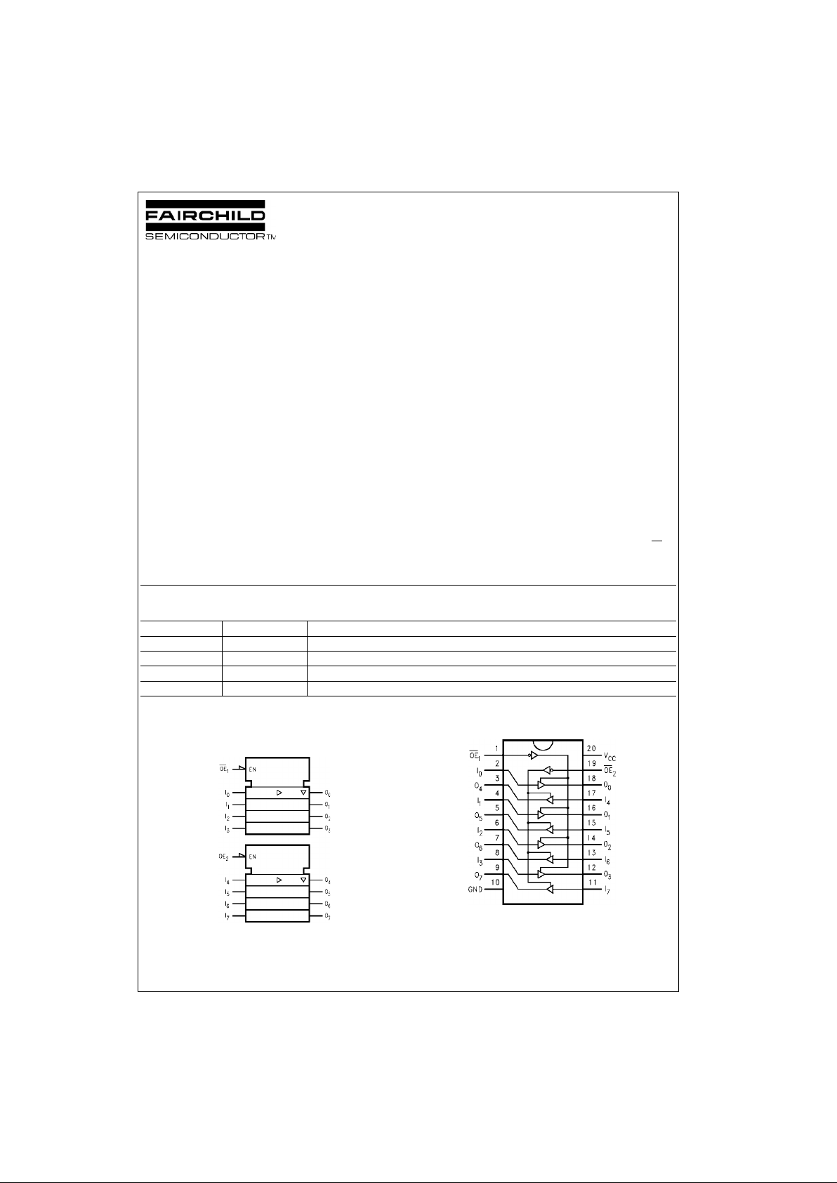
The LCX2244 contain s eight non-inverting bu ffers with 3STATE outputs. The device may be employed as a memory address driver, clock driver and bus-oriented transm itter/receiver. The LCX2244 is designed for low voltage
(2.5V or 3.3V) V
CC
applications with capability of interfac-
ing to a 5V signal envir onment. The 26Ω-series resistors
help reduce output overshoot and undershoot.
The LCX2244 is fabri cated with a n advanced CM OS technology to achieve high spee d operation while mai ntaining
CMOS low power dissipation.
Features
■ 5V tolerant inputs and outputs
■ 2.3V–3.6V V
CC
specifications provided
■ 7.5 ns t
PD
max (VCC = 3.3V) 10 µA ICC max
■ Power down high impedance inputs and outputs
■ 26Ω-series resistors in the outputs
■ Supports live insertion/withdrawal (Note 1)
■ ±12 mA output drive (V
CC
= 3.0V)
■ Implements patented noise/EMI reduction circuitry
■ Latch-up performance exceeds 500 mA
■ ESD performance:
Human body model > 2000V
Machine model > 200V
Note 1: To ensure the high-impedan c e state during power up or down, OE
should be tied to VCC through a pull-up res istor: the m inimu m value or t he
resistor is determin ed by the current-sourcing capability of the dr iv er.
Ordering Code:
Devices also availab le in Tape and Reel. Specify by appending su ffix let te r “X” to the ordering code.
Logic Symbol
IEEE/IEC
Connection Diagram
Order Number Package Number Package Description
74LCX2244WM M20B 20-Lead Small Outline Integrated Circuit (SOIC), JEDEC MS-013, 0.300” Wide
74LCX2244SJ M20D 20-Lead Small Outline Package (SOP), EIAJ TYPE II, 5.3mm Wide
74LCX2244MSA MSA20 20-Lead Shrink Small Outline Package (SSOP), EIAJ TYPE II, 5.3mm Wide
74LCX2244MTC MTC20 20-Lead Thin Shrink Small Outline Package (TSSOP), JEDEC MO-153, 4.4mm Wide

www.fairchildsemi.com 2
74LCX2244
Pin Descriptions
Truth Tables
H = HIGH Voltage Level
X = Immaterial
L = LOW Voltage Level
Z = High Impedance
Pin Names Description
OE
1
, OE
2
3-STATE Output Enable Inputs
I
0–I7
Inputs
O
0–O7
Outputs
Inputs Outputs
OE
1
I
n
(Pins 12, 14, 16, 18)
L L L
L H H
H X Z
Inputs Outputs
OE
2
I
n
(Pins 3, 5, 7, 9)
LH L
LH H
HX Z
3 www.fairchildsemi.com
74LCX2244
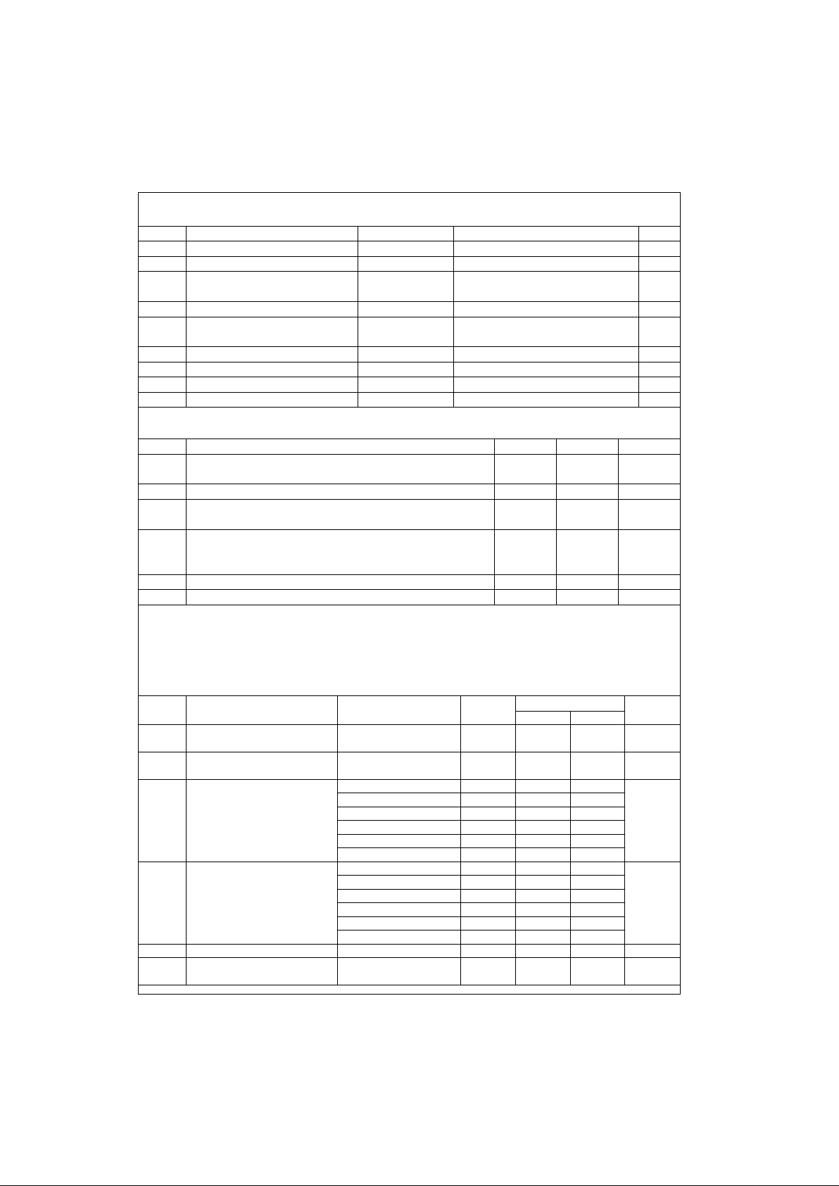
Absolute Maximum Ratings(Note 2)
Recommended Operating Conditions (Note 4)
Note 2: The Absolute Maximum Ratings are those values beyond which the safety of the device cannot be guaranteed. The device should not be operated
at these limits. The parametric values defined in the Electrical Characteristics tables are not guaranteed at the Absolute Maximum Ratings. The “Recommended Operating C onditions” table will def ine the conditions for actual device operation.
Note 3: I
O
Absolute Maximum Rating must be observed.
Note 4: Unused inputs must be held HIGH or LOW. They may not float.
DC Electrical Characteristics
Symbol Parameter Value Conditions Units
V
CC
Supply Voltage −0.5 to +7.0 V
V
I
DC Input Voltage −0.5 to +7.0 V
V
O
DC Output Voltage −0.5 to +7.0 Output in 3-STATE V
−0.5 to V
CC
+ 0.5 Output in HIGH or LOW State (Note 3)
I
IK
DC Input Diode Current −50 VI < GND mA
I
OK
DC Output Diode Current −50 VO < GND
mA
+50 V
O
> V
CC
I
O
DC Output Source/Sink Current ±50 mA
I
CC
DC Supply Current per Supply Pin ±100 mA
I
GND
DC Ground Current per Ground Pin ±100 mA
T
STG
Storage Temperature −65 to +150 °C
Symbol Parameter Min Max Units
V
CC
Supply Voltage Operating 2.0 3.6
V
Data Retention 1.5 3.6
V
I
Input Voltage 0 5.5 V
V
O
Output Voltage HIGH or LOW State 0 V
CC
V
3-STATE 0 5.5
I
OH/IOL
Output Current VCC = 3.0V − 3.6V ±12
mAV
CC
= 2.7V − 3.0V ±8
V
CC
= 2.3V − 2.7V ±4
T
A
Free-Air Operating Temperature −40 85 °C
∆t/∆V Input Edge Rate, V
IN
= 0.8V − 2.0V, VCC = 3.0V 0 10 ns/V
Symbol Parameter Conditions
V
CC
TA = −40°C to +85°C
Units
(V) Min Max
V
IH
HIGH Level Input Voltage 2.3 − 2.7 1.7
V
2.7 − 3.6 2.0
V
IL
LOW Level Input Voltage 2.3 − 2.7 0.7
V
2.7 − 3.6 0.8
V
OH
HIGH Level Output Voltage IOH = −100 µA2.3 − 3.6 VCC − 0.2
V
IOH = −4 mA 2.3 1.8
IOH = −4 mA 2.7 2.2
IOH = −6 mA 3.0 2.4
IOH = − 8mA 2.7 2.0
IOH = −12 mA 3.0 2.0
V
OL
LOW Level Output Voltage IOL = 100 µA2.3 − 3.6 0.2
V
IOL = 4 mA 2.3 0.6
IOL = 4 mA 2.7 0.4
IOL = 6 mA 3.0 0.55
IOL = 8 mA 2.7 0.6
IOL = 12 mA 3.0 0.8
I
I
Input Leakage Current 0 ≤ VI ≤ 5.5V 2.3 − 3.6 ±5.0 µA
I
OZ
3-STATE Output Leakage 0 ≤ VO ≤ 5.5V 2.3 − 3.6 ±5.0
µA
VI = VIH or V
IL
 Loading...