

Fairchild Semiconductor 74LCX16821MTDX, 74LCX16821MTD, 74LCX16821MEAX, 74LCX16821MEA, 74LCX16821CW Datasheet
January 1996
Revised April 1999
74LCX16821 Low Voltage 20-Bit D-Type Flip-Flop with 5V Tolerant Inputs and Outputs
© 1999 Fairchild Semiconductor Corporation DS012634.prf www.fairchildsemi.com
74LCX16821
Low Voltage 20-Bit D-Type Flip-Flop with 5V Tolerant
Inputs and Outputs
General Description
The LCX16821 contains twe nty non-inverting D-type flipflops with 3-STATE outputs and is intended for bus oriented
applications. The device is desi gned for low voltage (2.5V
or 3.3V) V
CC
applications with capability of interfacing to a
5V signal environment.
The LCX16821 is fabricated with an advanced CMOS tech-
nology to achieve high spee d operation while mai ntaining
CMOS low power dissipation.
Features
■ 5V tolerant inputs and outputs
■ 2.3V–3.6V V
CC
specifications provided
■ 6.2 ns t
PD
max (VCC = 3.3V), 20 µA ICC max
■ Power down high impedance inputs and outputs
■ Supports live insertion/withdrawal (Note 1)
■ ±24 mA output drive (V
CC
= 3.0V)
■ Implements patented noise/EMI reduction circuitry
■ Latch-up performance exceeds 500 mA
■ ESD performance:
Human body model > 2000V
Machine model > 200V
Note 1: To ensure the high-impedan c e state during power up or down, OE
should be tied to VCC through a pull-up res istor: the m inimu m value or t he
resistor is determin ed by the current-sourcing capability of the driver.
Ordering Code:
Devices also availab le in Tape and Reel. Specify by appending su ffix let te r “X” to the ordering code.
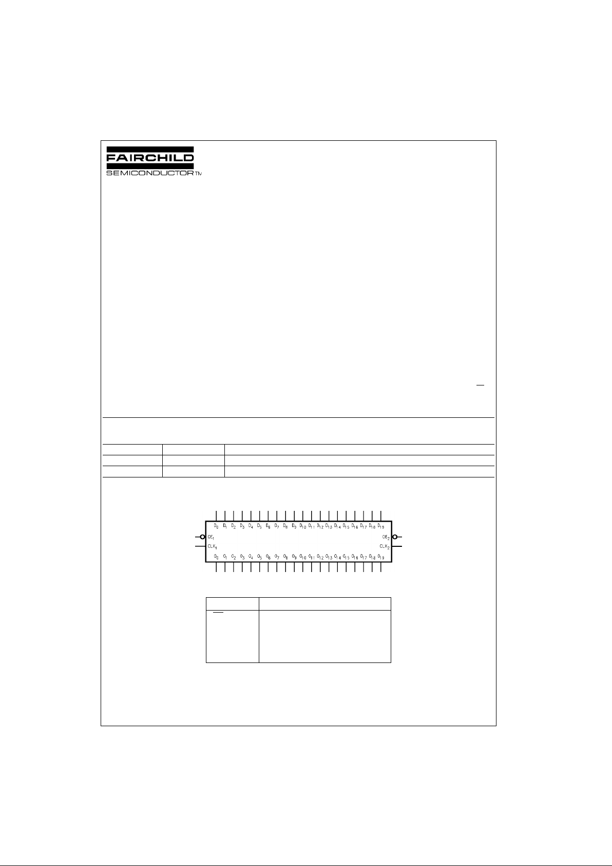
Logic Symbol
Pin Descriptions
Order Number Package Number Package Description
74LCX16821MEA MS56A 56-Lead Shrink Small Outline Package (SSOP), JEDEC MO-118, 0.300” Wide
74LCX16821MTD MTD56 56-Lead Thin Shrink Small Outline Package (TSSOP), JEDEC MO-153, 6.1mm Wide
Pin Names Description
OE
n
Output Enable Input (Active LOW)
CLK
n
Clock Input
D
0–D19
Inputs
O
0–O19
Outputs
www.fairchildsemi.com 2
74LCX16821
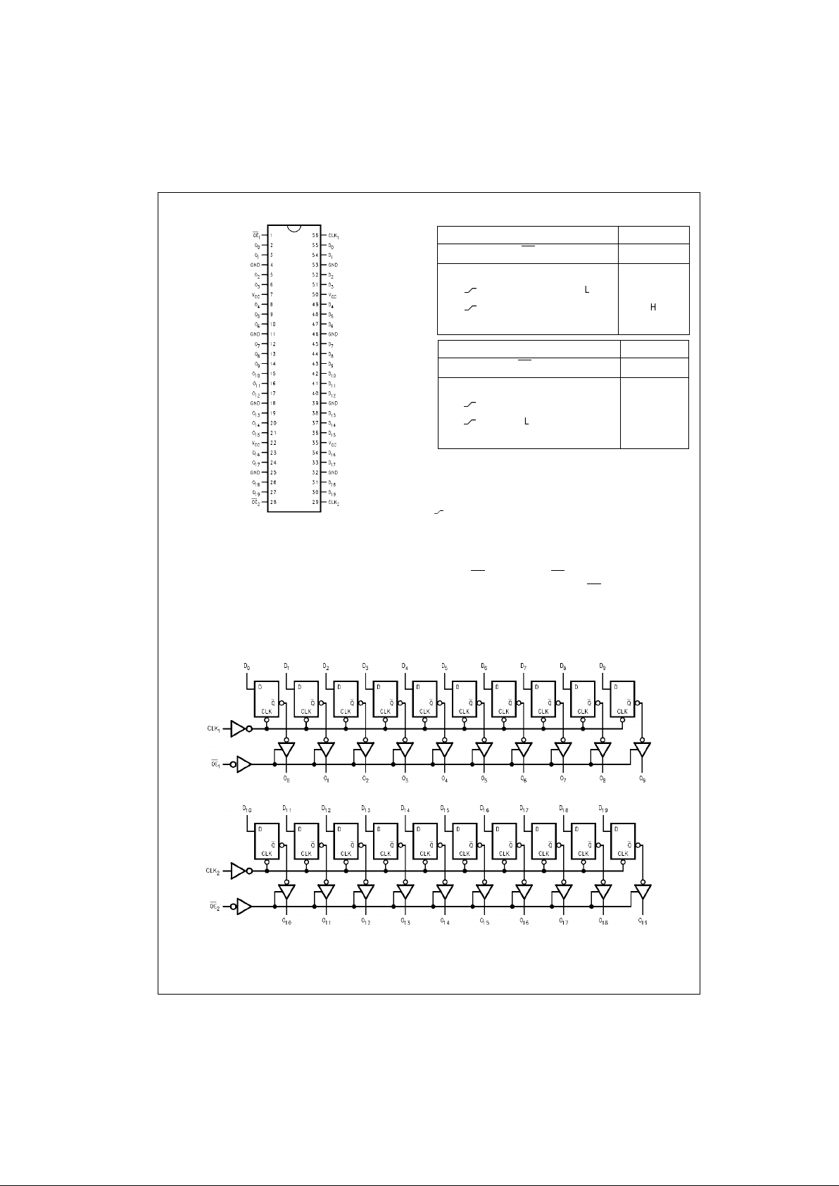
Connection Diagram Tr uth Tables
H = HIGH Voltage Level
L = LOW Voltage Level
X = Immaterial
Z = High Impedance
O
0
= Previous O0 before LOW-to-HIGH transition of Clock
= LOW-to-HIGH transition
Functional Description
The LCX16821 contains twenty D-type flip-flops with 3STATE standard outputs. The device is byte controlled with
each byte functioning identically, but independent of the
other. Control pins can be shorted together to obtai n full
20-bit operation. The following description applies to each
byte. The twenty flip-flops will store the state of their individual D inputs that meet the setup and hold time require-
ments on the LOW-to-HIGH Clock (CLK) transition. The 3STATE standard outputs are controlled by the Output
Enable (OE
n
) input. When OEn is LOW, the standard out-
puts are in the 2-state mode. When OE
n
is HIGH, the stan-
dard outputs are in the high impedance mode but this does
not interfere with entering new data into the flip-flops.
Logic Diagram
Please note that this diagram is provided only for the understan ding of logic operation s and should not be used t o es t im ate propagation delays.
Inputs Outputs
CLK
1
OE
1
D0–D
9
O0–O
9
XHX Z
LL L
LH H
L or H L X O
0
Inputs Outputs
CLK
2
OE
2
D10–D
19
O10–O
19
XH X Z
LL L
LH H
L or H L X O
0
3 www.fairchildsemi.com
74LCX16821
Absolute Maximum Ratings(Note 3)
Recommended Operating Conditions (Note 4)
Note 2: The Absolute Maximum Ratings are those values beyond which the safety of the device cannot be guaranteed. The device should not be operated
at these limits. The parametric values defined in the Electrical Characteristics tables are not guaranteed at the Absolute Maximum Ratings. The “Recommended Operating C onditions” table will def ine the conditions for ac t ual device operation.
Note 3: I
O
Absolute Maximum Rating must be observed.
Note 4: Unused pins (Inputs and I/O) must be held HIGH or LOW. They may not float.
DC Electrical Characteristics
Symbol Parameter Value Conditions Units
V
CC
Supply Voltage −0.5 to +7.0 V
V
I
DC Input Voltage −0.5 to +7.0 V
V
O
DC Output Voltage −0.5 to +7.0 Output in 3-STATE
V
−0.5 to V
CC
+ 0.5 Output in HIGH or LOW State (Note 3)
I
IK
DC Input Diode Current −50 VI < GND mA
I
OK
DC Output Diode Current −50 VO < GND
mA
+50 V
O
> V
CC
I
O
DC Output Source/Sink Current ±50 mA
I
CC
DC Supply Current per Supply Pin ±100 mA
I
GND
DC Ground Current per Ground Pin ±100 mA
T
STG
Storage Temperature −65 to +150 °C
Symbol Parameter Min Max Units
V
CC
Supply Voltage Operating 2.0 3.6
V
Data Retention 1.5 3.6
V
I
Input Voltage 0 5.5 V
V
O
Output Voltage HIGH or LOW State 0 V
CC
V
3-STATE 0 5.5
I
OH/IOL
Output Current VCC = 3.0V − 3.6V ±24
mAV
CC
= 2.7V − 3.0V ±12
V
CC
= 2.3V − 2.7V ±8
T
A
Free-Air Operating Temperature −40 85 °C
∆t/∆V Input Edge Rate, V
IN
= 0.8V – 2.0V, VCC = 3.0V 0 10 ns/V
Symbol Parameter
Conditions
V
CC
(V)
TA = −40°C to +85°C
Units
Min Max
V
IH
HIGH Level Input Voltage 2.3 − 2.7 1.7
V
2.7 − 3.6 2.0
V
IL
LOW Level Input Voltage 2.3 − 2.7 0.7
V
2.7 − 3.6 0.8
V
OH
HIGH Level Output Voltage IOH = −100 µA2.3 − 3.6 VCC − 0.2
V
IOH = −8 mA 2.3 1.8
IOH = −12 mA 2.7 2.2
IOH = −18 mA 3.0 2.4
IOH = −24 mA 3.0 2.2
V
OL
LOW Level Output Voltage IOL = 100 µA2.3 − 3.6 0.2
V
IOL = 8 mA 2.3 0.6
IOL = 12 mA 2.7 0.4
IOL = 16 mA 3.0 0.4
IOL = 24 mA 3.0 0.55
I
I
Input Leakage Current 0 ≤ VI ≤ 5.5V 2.3 − 3.6 ±5.0 µA
I
OZ
3-STATE Output Leakage 0 ≤ VO ≤ 5.5V 2.3 − 3.6 ±5.0
µA
VI = VIH or V
IL
I
OFF
Power-Off Leakage Current VI or VO = 5.5V 0 10 µA
 Loading...