

Fairchild Semiconductor 74LCX16646MTDX, 74LCX16646MTD, 74LCX16646MEAX, 74LCX16646MEA, 74LCX16646CW Datasheet
February 1994
Revised April 1999
74LCX16646 Low Voltage 16-Bit Transceiver/Register with 5V Tolerant Inputs and Outputs
© 1999 Fairchild Semiconductor Corporation DS012004.prf www.fairchildsemi.com
74LCX16646
Low Voltage 16-Bit Transceiver/Register with 5V Tolerant
Inputs and Outputs
General Description
The LCX16646 conta ins s ixteen n on-inve rting bidir ectional
registered bus transce ivers with 3-STATE outputs, providing multiplexed transmission of data directly from the input
bus or from the i nternal storage reg isters. Each byte has
separate control inputs which can be shorted tog ether for
full 16-bit operation.The DIR inputs determine the direction
of data flow through the device. The CPAB and CPBA
inputs load data into the registers on the LOW-to-HIGH
transition (see Functional Description).
The LCX16646 is desi gned for low vol tage (2.5V or 3.3V )
V
CC
applications with capability of interfacing to a 5V signal
environment.
The LCX16646 is fabricated with an advanced CMOS tech-
nology to achieve high spee d operation while mai ntaining
CMOS low power dissipation.
Features
■ 5V tolerant inputs and outputs
■ 2.3V–3.6V V
CC
specifications provided
■ 5.2 ns t
PD
max (VCC = 3.3V), 20 µA ICC max
■ Power down high impedance inputs and outputs
■ Supports live insertion/withdrawal (Note 1)
■ ±24 mA Output Drive (V
CC
= 3.0V)
■ Implements patented noise/EMI reduction circuitry
■ Latch-up performance exceeds 500 mA
■ ESD performance:
Human Body Model > 2000V
Machine Model > 200V
Note 1: To ensure the high-impedan c e state during power up or down, OE
should be tied to VCC through a pull-up res istor: the m inimu m value or t he
resistor is determin ed by the current-sourcing capability of the dr iv er.
Ordering Code:
Devices also availab le in Tape and Reel. Specify by appending su ffix let te r “X” to the ordering code.
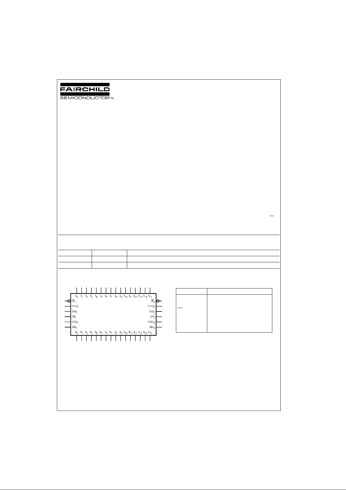
Logic Symbol Pin Descriptions
Order Number Package Number Package Description
74LCX16646MEA MS56A 56-Lead Shrink Small Outline Package (SSOP), JEDEC MO-118, 0.300” Wide
74LCX16646MTD MTD56 56-Lead Thin Shrink Small Outline Package (TSSOP), JEDEC MO-153, 6.1mm Wide
Pin Names Description
A
n
Side A Inputs or 3-STATE Outputs
B
n
Side B Inputs or 3-STATE Outputs
OE
n
Output Enable Inputs
CPAB
n
, CPBAnClock Pulse Inputs
SAB
n
, SBAnSelect Inputs
DIR
n
Direction Control Inputs
www.fairchildsemi.com 2
74LCX16646
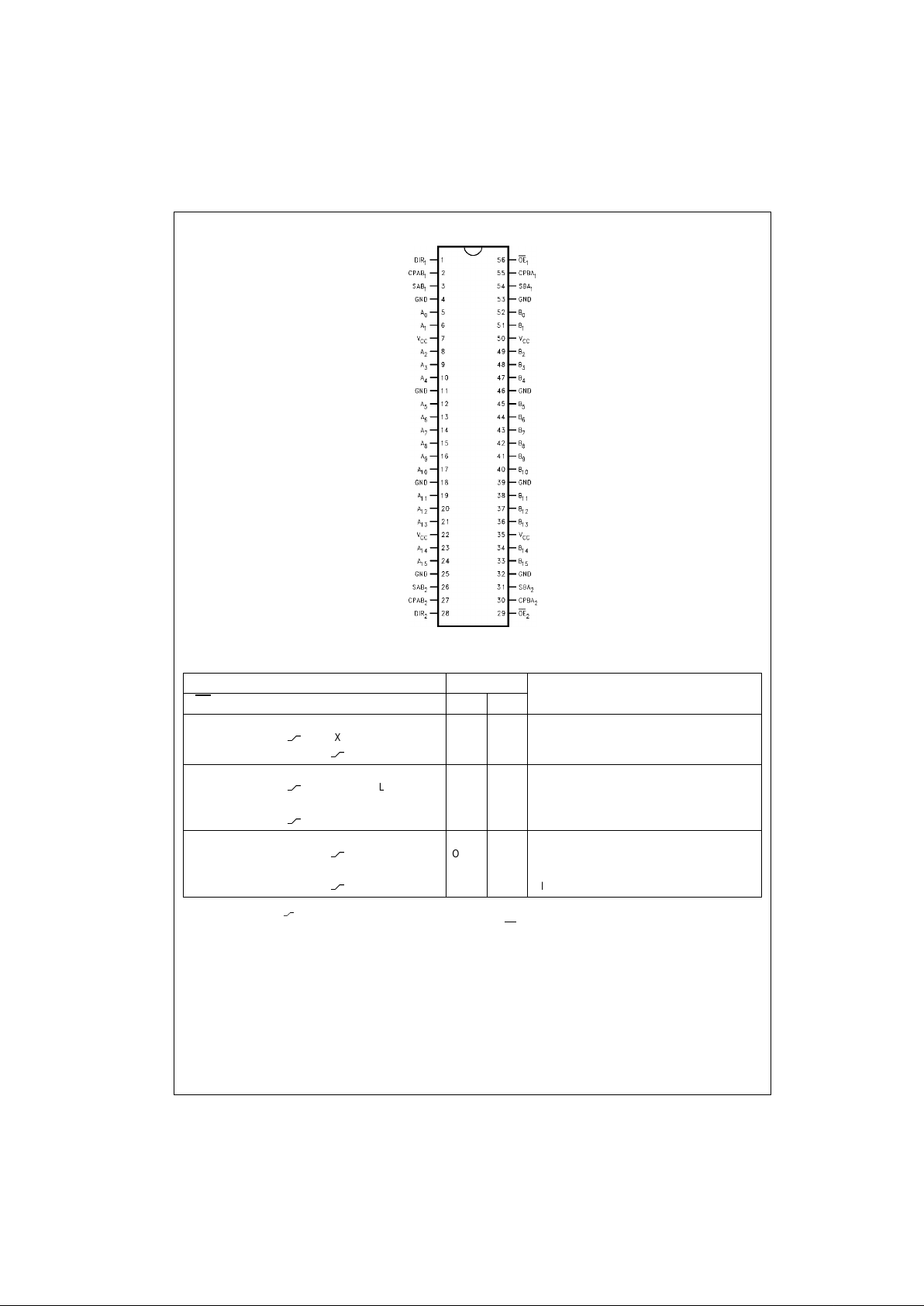
Connection Diagram
Truth Table
(Note 2)
H = HIGH Voltage Level X = Immaterial
L = LOW Voltage Level
= LOW-to-HIGH Transition.
Note 2: The data output functions may be enabled or disabled by various signals at the OE
and DIR inputs. Data in put functions are alway s enabled;
i.e., data at the bus pins w ill be stored on every LOW-to-HIGH transition of the appropriate clock inputs. Also applies to data I/O (A and B: 8-15) and #2 control pins.
Inputs Data I/O
Output Operation Mode
OE
1
DIR1 CPAB1 CPBA1 SAB1 SBA1 A
0–7 B0–7
H X H or L H or L X X Isolation
H X
X X X Input Input Clock An Data into A Register
H X X
X X Clock Bn Data Into B Register
L H X X L X A
n
to Bn—Real Time (Transparent Mode)
L H
X L X Input Output Clock An Data to A Register
L H H or L X H X A Register to B
n
(Stored Mode)
L H
X H X Clock An Data into A Register and Output to B
n
L L X X X L Bn to An—Real Time (Transparent Mode)
L L X
X L Output Input Clock Bn Data into B Register
L L X H or L X H B Register to A
n
(Stored Mode)
L L X
X H Clock Bn into B Register and Output to A
n
3 www.fairchildsemi.com
74LCX16646
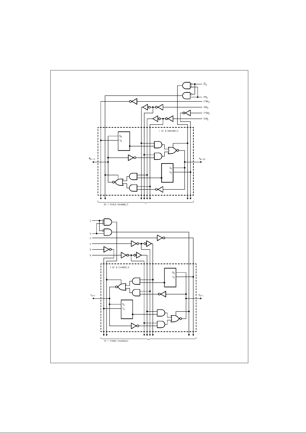
Logic Diagrams
Please note that thes e diagrams are provide d only for the understan ding of logic operations a nd should not be used to es t im ate propagation delays.
 Loading...