


Fairchild Semiconductor 74LCX16543MTDX, 74LCX16543MTD, 74LCX16543MEAX, 74LCX16543MEA, 74LCX16543CW Datasheet
May 1995
Revised April 1999
74LCX16543 Low Voltage 16-Bit Registered Transceiver with 5V Tolerant Inputs and Outputs
© 1999 Fairchild Semiconductor Corporation DS012464.prf www.fairchildsemi.com
74LCX16543
Low Voltage 16-Bit Registered Transceiver with
5V Tolerant Inputs and Outputs
General Description
The LCX16543 contains sixteen no n-inver ting tran sceive rs
containing two sets of D-type registe rs for temporary storage of data flowing in either dir ecti o n. Each byte ha s sep arate control inputs wh ich can be shorted together for full
16-bit operation. Separate Latch Enable and Output
Enable inputs are provided for each register to permit independent input and o utput contr ol in either directio n of data
flow.
The LCX16543 is desi gned for low vol tage (2.5V or 3.3V )
V
CC
applications with capability of interfacing to a 5V signal
environment.
The LCX16543 is fabricated with an advanced CMOS tech-
nology to achieve high spee d operation while mai ntaining
CMOS low power dissipation.
Features
■ 5V tolerant inputs and outputs
■ 2.3V–3.6V V
CC
specifications provided
■ 5.2 ns t
PD
max (VCC = 3.3V), 20 µA ICC max
■ Power down high impedance inputs and outputs
■ Supports live insertion/withdrawal (Note 1)
■ ±24 mA Output Drive (V
CC
= 3.0V)
■ Implements patented noise/EMI reduction circuitry
■ Latch-up performance exceeds 500 mA
■ ESD performance:
Human Body Model > 200 0V
Machine Model > 200V
Note 1: To ensure the high-impedan c e state during power up or down, OE
should be tied to VCC through a pull-up res istor: the m inimu m value or t he
resistor is determin ed by the current-sourcin g c apability of the driver.
Ordering Code:
Devices also availab le in Tape and Reel. Specify by appending th e s uffix let t er “X” to the ordering code.
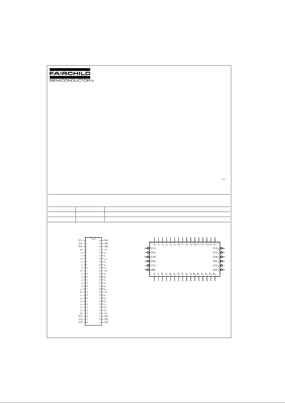
Connection Diagram Logic Symbol
Order Number Package Number Package Description
74LCX16543MEA MS56A 56-Lead Small Shrink Outline Package (SSOP), JEDEC MO-118, 0.300” Wide
74LCX16543MTD MTD56 56-Lead Thin Shrink Small Outline Package (TSSOP), JEDEC MO-153, 6.1mm Wide
www.fairchildsemi.com 2
74LCX16543
Pin Descriptions
Data I/O Control Table
H = HIGH Voltage Level
L = LOW Voltage Level
X = Immaterial
A-to-B data flow shown; B-to-A flow control is the same, except using CEBA
n
, LEBAn and OEBA
n
Functional Description
The LCX16543 contains sixtee n non-i nvert ing tran sceivers
with 3-STATE outputs. The device is b yte controlled with
each byte functioning identically, but independent of the
other. The control pins may be shorted together to obta in
full 16-bit operat ion. The following description applies to
each byte. For data flow from A to B, for example, the A-toB Enable (CEAB
n
) input must be LOW in or der to enter
data from A
0–A15
or take data from B0–B15, as indicated in
the Data I/O Control Table. With CEAB
n
LOW, a LOW sig-
nal on the A-to-B Latch Enable (LEAB
n
) input makes the A-
to-B latches transparent; a subsequent LOW-to-HIGH transition of the LEAB
n
signal puts the A latches i n th e st ora ge
mode and their outputs no longer change with the A inputs.
With CEAB
n
and OEABn both LOW, the 3-STATE B output
buffers are active and reflect the data present at the output
of the A latches. Control of data flow from B to A is simil ar,
but using the CEBA
n
, LEBAn and OEBAn inputs.
Pin Names Description
OEAB
n
A-to-B Output Enable Input (Active LOW)
OEBA
n
B-to-A Output Enable Input (Active LOW)
CEAB
n
A-to-B Enable Input (Active LOW)
CEBA
n
B-to-A Enable Input (Active LOW)
LEAB
n
A-to-B Latch Enable Input (Active LOW)
LEBA
n
B-to-A Latch Enable Input (Active LOW)
A
0–A15
A-to-B Data Inputs or B-to-A 3-STATE Outputs
B
0–B15
B-to-A Data Inputs or A-to-B 3-STATE Outputs
Inputs Latch
Status
Output
Buffers
CEAB
n
LEABnOEABn(Byte n) (Byte n)
H X X Latched High Z
X H X Latched —
L L X Transparent —
X X H — High Z
L X L — Driving
3 www.fairchildsemi.com
74LCX16543
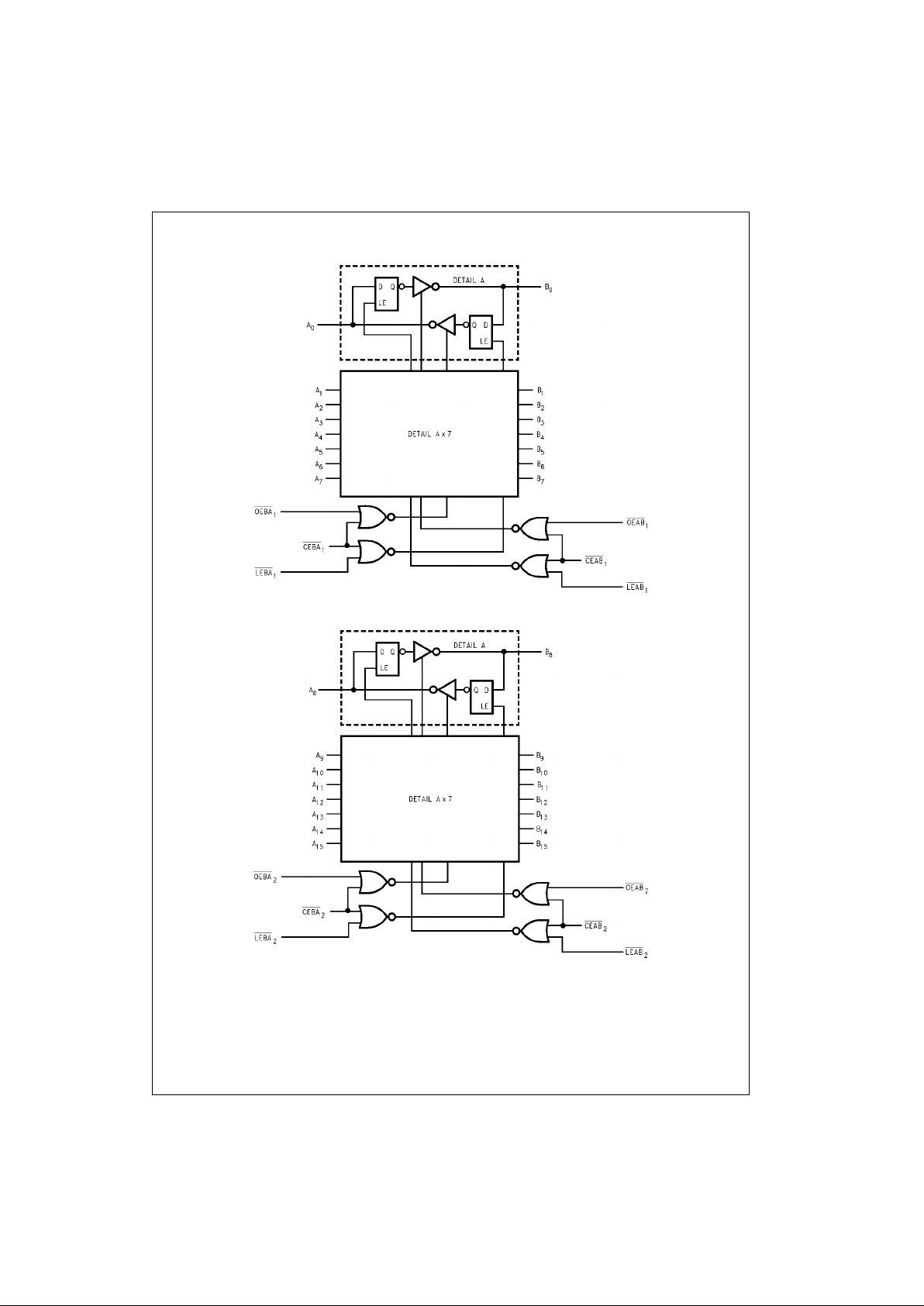
Logic Diagrams
Byte 1 (0:7)
Please note that this d iagram is provided only for t he understanding of lo gic operations and should not be used to estimate propagation delays.
Byte 2 (8:15)
Please note that this d iagram is provided only for t he understanding of lo gic operations and should not be used to estimate propagation delays.