

Fairchild Semiconductor 74LCX16374MTDX, 74LCX16374MEAX, 74LCX16374MEA, 74LCX16374CW Datasheet
February 1994
Revised April 1999
74LCX16374 Low Voltage 16-Bit D-Type Flip-Flop with 5V Tolerant Inputs and Outputs
© 1999 Fairchild Semiconductor Corporation DS012003.prf www.fairchildsemi.com
74LCX16374
Low Voltage 16-Bit D-Type Flip-Flop with 5V Tolerant
Inputs and Outputs
General Description
The LCX16374 contains sixteen non-inverting D-type flipflops with 3-STATE outputs and is intended for bus oriented
applications. The device is byte controlled. A buffered clock
(CP) and Output En able (OE
) are common to each byte
and can be shorted together for full 16-bit operation.
The LCX16374 is desi gned for low vol tage (2.5V or 3.3V )
V
CC
applications with capability of interfacing to a 5V signal
environment.
The LCX16374 is fabricated with an advanced CMOS tech-
nology to achieve high spee d operation while mai ntaining
CMOS low power dissipation.
Features
■ 5V tolerant inputs and outputs
■ 2.3V–3.6V V
CC
specifications provided
■ 6.2 ns t
PD
max (VCC = 3.3V), 20 µA ICC max
■ Power down high impedance inputs and outputs
■ Supports live insertion/withdrawal (Note 1)
■ ±24 mA output drive (V
CC
= 3.0V)
■ Implements patented noise/EMI reduction circuitry
■ Latch-up performance exceeds 500 mA
■ ESD performance:
Human body model > 2000V
Machine model > 200V
Note 1: To ensure the high-impedan c e state during power up or down, OE
should be tied to VCC through a pull-up res istor: the m inimu m value or t he
resistor is determin ed by the current-sourcing capability of the driver.
Ordering Code:
Devices also availab le in Tape and Reel. Specify by appending th e s uffix let t er “X” to the ordering code.
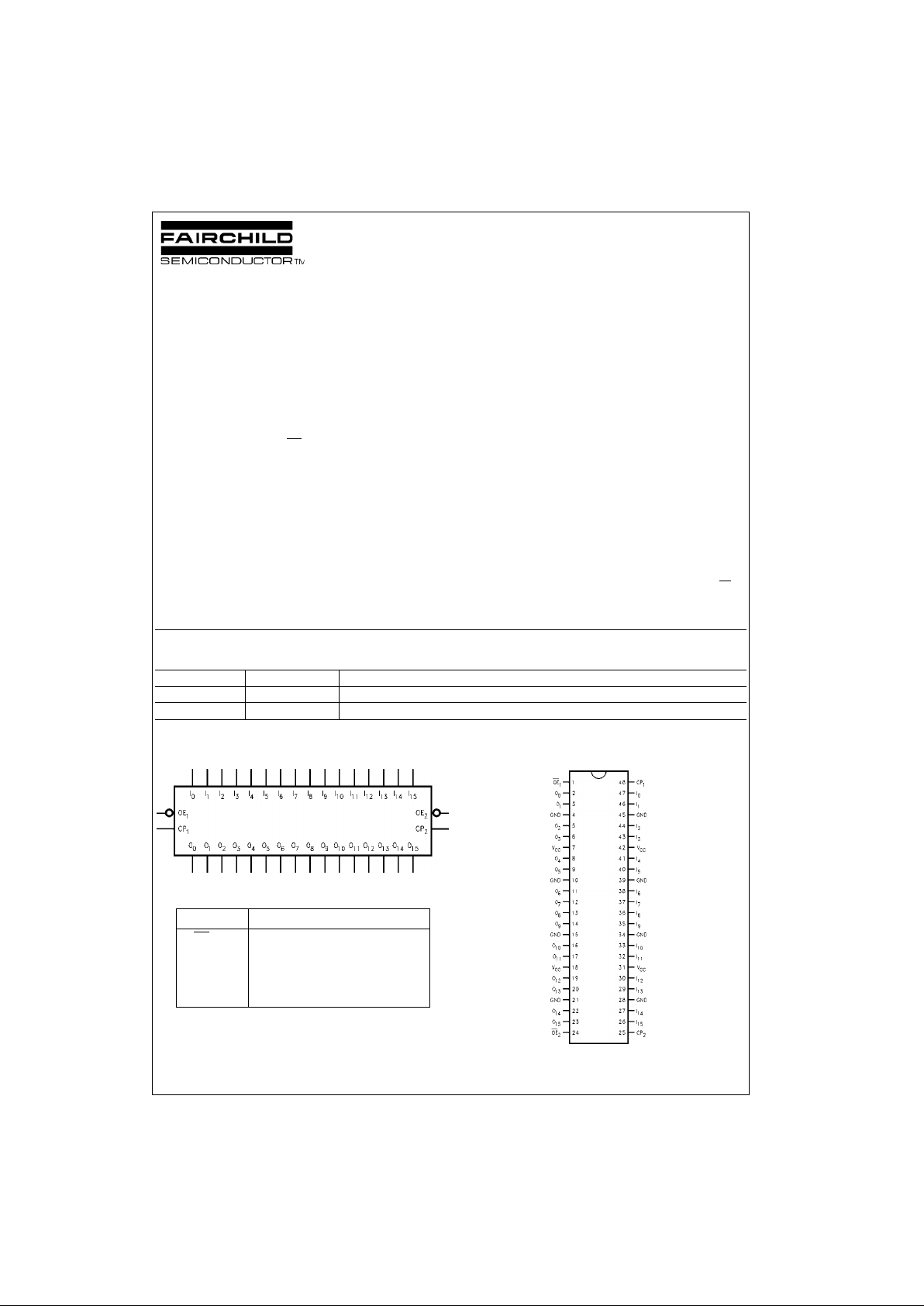
Logic Symbol
Pin Descriptions
Connection Diagram
Order Number Package Number Package Description
74LCX16374MEA MS48A 48-Lead Small Shrink Outline Package (SSOP), JEDEC MO-118, 0.300” Wide
74LCX16374MTD MTD48 48-Lead Thin Shrink Small Outline Package (TSSOP), JEDEC MO-153, 6.1mm Wide
Pin Names Description
OE
n
Output Enable Input (Active LOW)
CP
n
Clock Pulse Input
I
0–I15
Inputs
O
0–O15
Outputs
www.fairchildsemi.com 2
74LCX16374
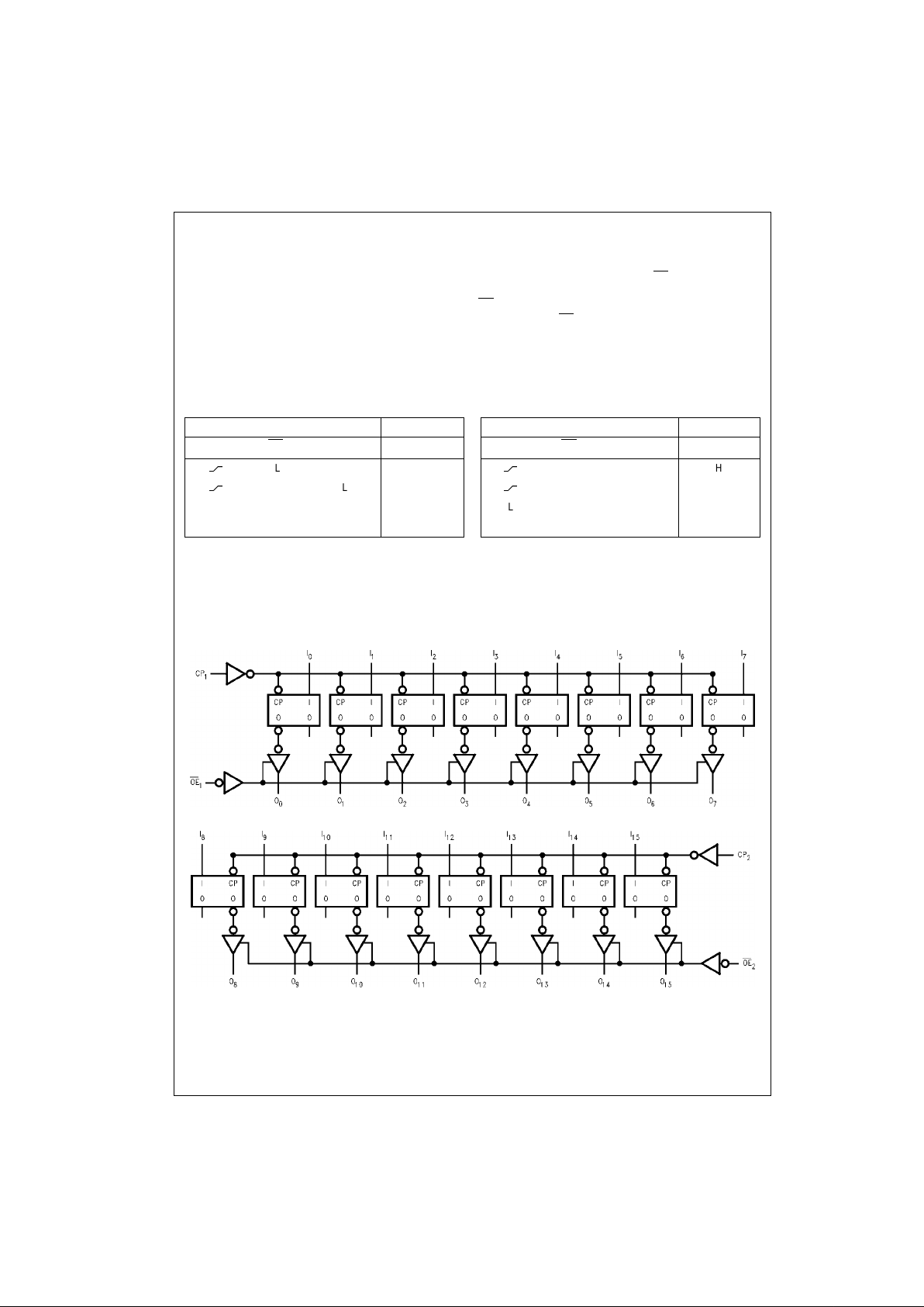
Functional Description
The LCX16374 consists of sixteen edge-triggered flip-flops
with individual D-type inputs and 3-STATE true outputs.
The device is byte controlled with each byte functionin g
identically, but independent of the ot her. The control pins
can be shorted together to obtain full 16-bit operation.
Each byte has a buffered clock and buffered Output Enable
common to all flip-flo ps within that byte. The description
which follows applies to each byte. Each flip-flop will store
the state of their individual D inputs that meet the setup and
hold time requiremen ts on the LOW-to-HIGH Clo ck (CP
n
)
transition. With the Output Enable (OE
n
) LOW, the con-
tents of the flip-flops are ava ilable at the outputs. When
OE
n
is HIGH, the outputs go to the high impedan ce state.
Operation of the OE
n
input does not affect the state of the
flip-flops.
Truth Tables
H = HIGH Voltage Level
L = LOW Voltage Level
X = Immaterial
Z = High Impedance
O0 = Previous O0 before HIGH-to-LOW of CP
Logic Diagrams
Byte 1 (0:7)
Byte 2 (8:15)
Please note that this diagram is provided only for the understan ding of logic operation s and should not be used t o es t im ate propagation delays.
Inputs Outputs
CP
1
OE
1
I0–I
7
O0–O
7
LH H
LL L
LL X O
0
XH X Z
Inputs Outputs
CP
2
OE
2
I8–I
15
O8–O
15
LH H
LL L
LL X O
0
XH X Z
3 www.fairchildsemi.com
74LCX16374
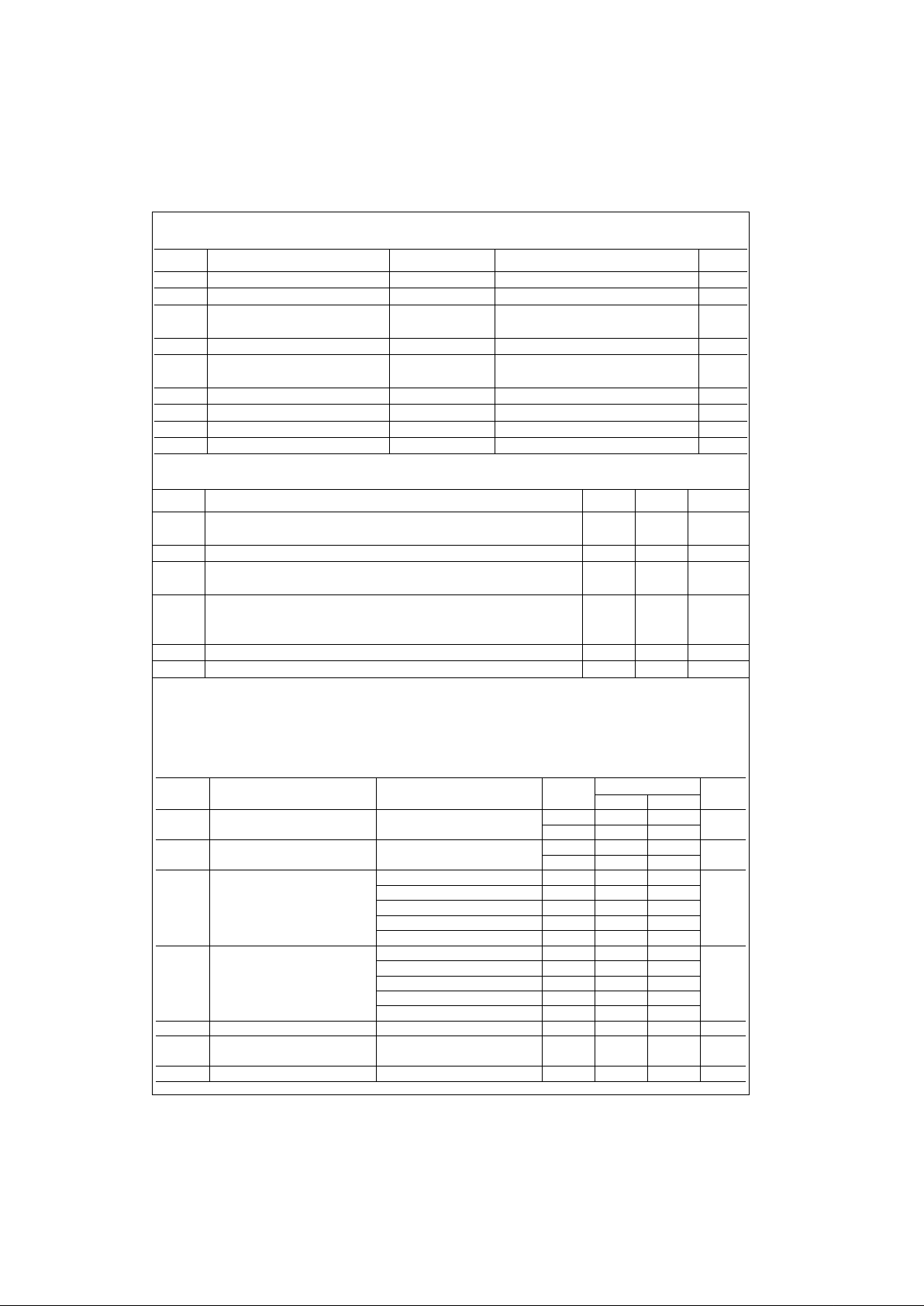
Absolute Maximum Ratings(Note 2)
Recommended Operating Conditions (Note 4)
Note 2: The Absolute Maximum Ratings are those values beyond which the safety of the device cannot be guaranteed. The device should not be operated
at these limits. The parametric values defined in the Electrical Characteristics tables are not guaranteed at the Absolute Maximum Ratings. The “Recommended Operating C onditions” table will def ine the conditions for ac t ual device operation.
Note 3: I
O
Absolute Maximum Rating must be observed.
Note 4: Unused inputs must be held HIGH or LOW. They may not float.
DC Electrical Characteristics
Symbol Parameter Value Conditions Units
V
CC
Supply Voltage −0.5 to +7.0 V
V
I
DC Input Voltage −0.5 to +7.0 V
V
O
DC Output Voltage −0.5 to +7.0 3-STATE
V
−0.5 to V
CC
+ 0.5 Output in HIGH or LOW State (Note 3)
I
IK
DC Input Diode Current −50 VI < GND mA
I
OK
DC Output Diode Current −50 VO < GND
mA
+50 V
O
> V
CC
I
O
DC Output Source/Sink Current ±50 mA
I
CC
DC Supply Current per Supply Pin ±100 mA
I
GND
DC Ground Current per Ground Pin ±100 mA
T
STG
Storage Temperature −65 to +150 °C
Symbol Parameter Min Max Units
V
CC
Supply Voltage Operating 2.0 3.6
V
Data Retention 1.5 3.6
V
I
Input Voltage 0 5.5 V
V
O
Output Voltage HIGH or LOW State 0 V
CC
V
3-STATE 0 5.5
I
OH/IOL
Output Current VCC = 3.0V − 3.6V ±24
mAV
CC
= 2.7V − 3.0V ±12
V
CC
= 2.3V − 2.7V ±8
T
A
Free-Air Operating Temperature −40 85 °C
∆t/∆V Input Edge Rate, V
IN
= 0.8V–2.0V, VCC = 3.0V 0 10 ns/V
Symbol Parameter Conditions
V
CC
TA = −40°C to +85°C
Units
(V) Min Max
V
IH
HIGH Level Input Voltage 2.3 − 2.7 1.7
V
2.7 − 3.6 2.0
V
IL
LOW Level Input Voltage 2.3 − 2.7 0.7
V
2.7 − 3.6 0.8
V
OH
HIGH Level Output Voltage IOH = −100 µA2.3 − 3.6 VCC − 0.2
V
IOH = −8 mA 2.3 1.8
IOH = −12 mA 2.7 2.2
IOH = −18 mA 3.0 2.4
IOH = −24 mA 3.0 2.2
V
OL
LOW Level Output Voltage IOL = 100 µA2.3 − 3.6 0.2
V
IOL = 8 mA 2.3 0.6
IOL = 12 mA 2.7 0.4
IOL = 16 mA 3.0 0.4
IOL = 24 mA 3.0 0.55
I
I
Input Leakage Current 0 ≤ VI ≤ 5.5V 2.3 − 3.6 ±5.0 µA
I
OZ
3-STATE Output Leakage 0 ≤ VO ≤ 5.5V 2.3 − 3.6 ±5.0
µA
VI = VIH or V
IL
I
OFF
Power-Off Leakage Current VI or VO = 5.5V 0 10 µA
 Loading...