

Fairchild Semiconductor 74LCX16245MTDX, 74LCX16245MTD, 74LCX16245MEAX, 74LCX16245MEA, 74LCX16245CW Datasheet
© 2000 Fairchild Semiconductor Corporation DS012001 www.fairchildsemi.com
February 1994
Revised April 2000
74LCX16245 Low Voltage 16-Bit Bidirectional Transceiver with 5V Tolerant Inputs and Outputs
74LCX16245
Low Voltage 16-Bit Bidirectional Transceiver with
5V Tolerant Inputs and Outputs
General Description
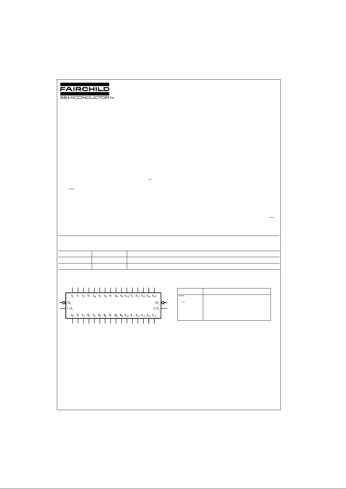
The LCX16245 conta ins s ixteen n on-i nvertin g bidi rectio nal
buffers with 3-STATE outputs and is in tended for bus oriented applications. The device is designed for lo w voltage
(2.5V or 3.3V) V
CC
applications with capability of interfac-
ing to a 5V signal environment. The device is byte controlled. Each byte has sepa rate control inputs which co uld
be shorted together for full 16-bi t ope ra tion. The T/R
inputs
determine the dire ction of data flow through the de vice.
The OE
inputs disable bo th the A and B ports by placing
them in a high impedance state.
The LCX16245 is fabricated with an advanced CMOS tech-
nology to achieve high s peed operation while maintaining
CMOS low power dissipation.
Features
■ 5V tolerant inputs and outputs
■ 2.3V–3.6V V
CC
specifications provided
■ 4.5 ns t
PD
max (VCC = 3.3V), 20 µA ICC max
■ Power down high impedance inputs and outputs
■ Supports live insertion/withdrawal (Note 1)
■ ±24 mA output drive (V
CC
= 3.0V)
■ Implements patented noise/EMI reduction circuitry
■ Latch-up performance exce eds 500 mA
■ ESD performance:
Human body model > 2000V
Machine model > 200V
Note 1: To ensure the high-impedance state during power up or down, OE
should be tied to VCC through a pull-up res istor: the m inimu m value or t he
resistor is determin ed by the current-sourcin g c apability of the driver.
Ordering Code:
Devices also availab le in Tape and Reel. Specify by appending th e s uffix let t er “X” to the ordering code.
Logic Symbol Pin Descriptions
Order Number Package Number Package Description
74LCX16245MEA MS48A 48-Lead Small Shrink Outline Package (SSOP), JEDEC MO-118, 0.300” Wide
74LCX16245MTD MTD48 48-Lead Thin Shrink Small Outline Package (TSSOP), JEDEC MO-153, 6.1mm Wide
Pin Names Description
OE
n
Output Enable Input
T/R
n
Transmit/Receive Input
A
0–A15
Side A Inputs or 3-STATE Outputs
B
0–B15
Side B Inputs or 3-STATE Outputs
www.fairchildsemi.com 2
74LCX16245
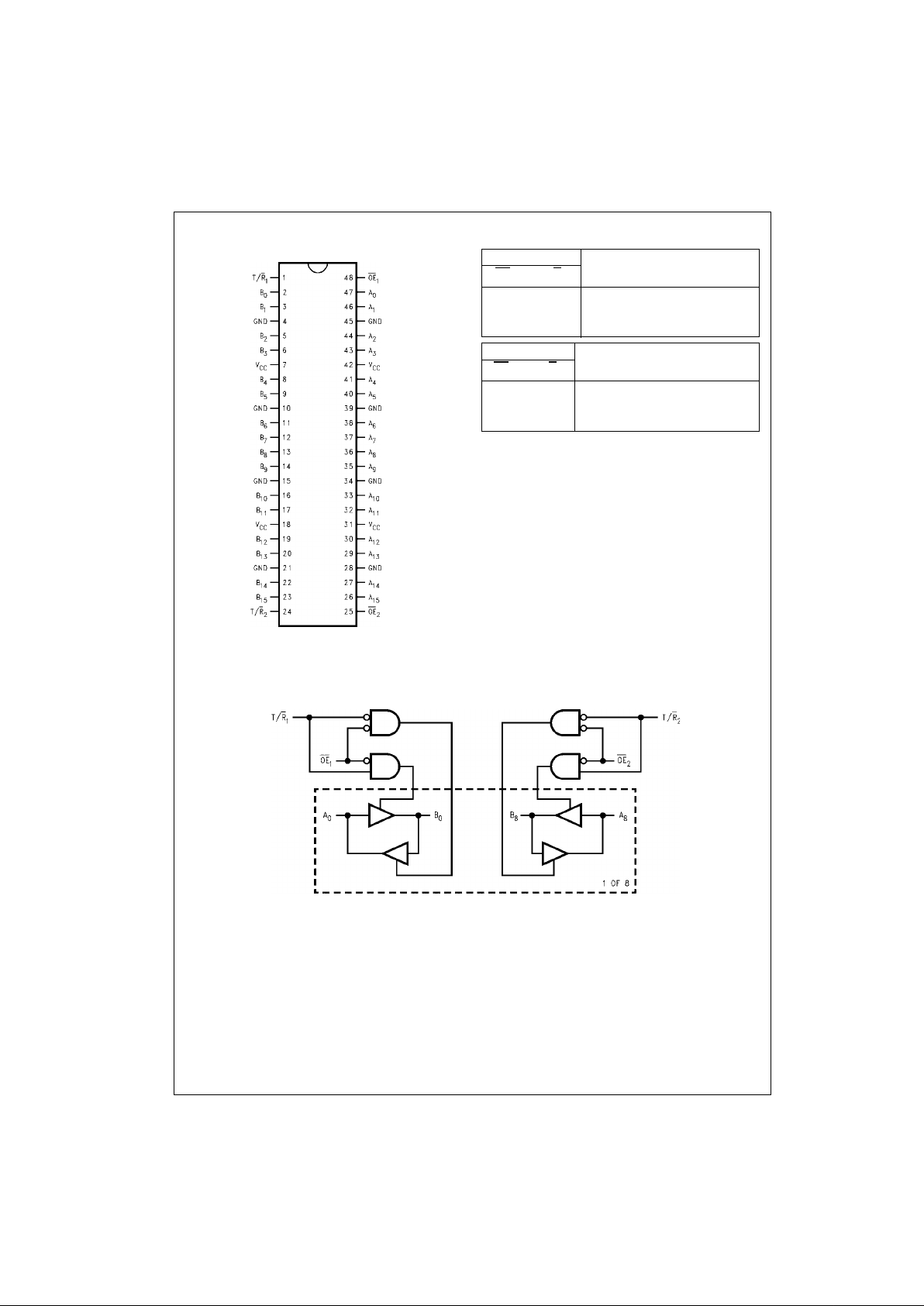
Connection Diagram Tr uth Tables
H = HIGH Voltage Level
L = LOW Voltage Level
X = Immaterial
Z = High Impedance
Logic Diagram
Inputs
Outputs
OE
1
T/R
1
LLBus B
0–B7
Data to Bus A0–A
7
LHBus A
0–A7
Data to Bus B0–B
7
H X HIGH Z State on A0–A7, B0–B
7
Inputs
Outputs
OE
2
T/R
2
L L Bus B8–B15 Data to Bus A8–A
15
L H Bus A8–A15 Data to Bus B8–B
15
H X HIGH Z State on A8–A15, B8–B
15
3 www.fairchildsemi.com
74LCX16245
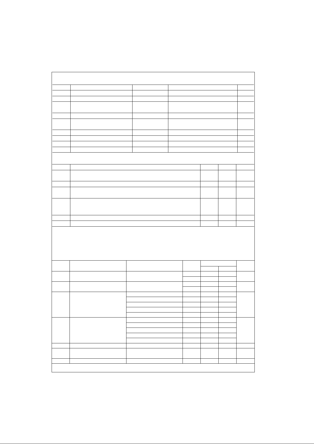
Absolute Maximum Ratings(Note 2)
Recommended Operating Conditions (Note 4)
Note 2: The Absolute Maximum Ratings are those values beyond which the safety of the device cannot be guaranteed. The device should not be operated
at these limits. The parametric values defined in the Electrical Characteristics tables are not guaranteed at the Absolute Maximum Ratings. The “Recom-
mended Operating Conditions” table will define the conditions for actual device operation.
Note 3: I
O
Absolute Maximum Rating must be observed.
Note 4: Unused inputs or I/O's mus t be held HIGH or LOW. They may no t flo at .
DC Electrical Characteristics
Symbol Parameter Value Conditions Units
V
CC
Supply Voltage −0.5 to +7.0 V
V
I
DC Input Voltage −0.5 to +7.0 V
V
O
DC Output Voltage −0.5 to +7.0 Output in 3-ST ATE
V
−0.5 to V
CC
+ 0.5 Output in HIGH or LOW State (Note 3)
I
IK
DC Input Diode Current −50 VI < GND mA
I
OK
DC Output Diode Current −50 VO < GND
mA
+50 V
O
> V
CC
I
O
DC Output Source/Sink Current ±50 mA
I
CC
DC Supply Current per Supply Pin ±100 mA
I
GND
DC Ground Current per Ground Pin ±100 mA
T
STG
Storage Temperature −65 to +150 °C
Symbol Parameter Min Max Units
V
CC
Supply Voltage Operating 2.0 3.6
V
Data Retention 1.5 3.6
V
I
Input Voltage 05.5V
V
O
Output Voltage HIGH or LOW State 0 V
CC
V
3-STATE 0 5.5
I
OH/IOL
Output Current VCC = 3.0V − 3.6V ±24
mAV
CC
= 2.7V − 3.0V ±12
V
CC
= 2.3V − 2.7V ±8
T
A
Free-Air Operating Temperature −40 85 °C
∆t/∆V Input Edge Rate, V
IN
= 0.8V–2.0V, VCC = 3.0V 0 10 ns/V
Symbol Parameter Conditions
V
CC
TA = −40°C to +85°C
Units
(V) Min Max
V
IH
HIGH Level Input Voltage 2.3 − 2.7 1.7
V
2.7 − 3.6 2.0
V
IL
LOW Level Input Voltage 2.3 − 2.7 0.7
V
2.7 − 3.6 0.8
V
OH
HIGH Level Output Voltage IOH = −100 µA2.3 − 3.6 VCC − 0.2
V
IOH = −8 mA 2.3 1.8
IOH = −12 mA 2.7 2.2
IOH = −18 mA 3.0 2.4
IOH = −24 mA 3.0 2.2
V
OL
LOW Level Output Voltage IOL = 100 µA2.3 − 3.6 0.2
V
IOL = 8mA 2.3 0.6
IOL = 12 mA 2.7 0.4
IOL = 16 mA 3.0 0.4
IOL = 24 mA 3.0 0.55
I
I
Input Leakage Current 0 ≤ VI ≤ 5.5V 2.3 − 3.6 ±5.0 µA
I
OZ
3-STATE I/O Leakage 0 ≤ VO ≤ 5.5V 2.3 − 3.6 ±5.0
µA
VI = VIH or V
IL
I
OFF
Power-Off Leakage Current VI or VO = 5.5V 0 10 µA
 Loading...