

Fairchild Semiconductor 74LCX16244MTDX, 74LCX16244MTD, 74LCX16244MEAX, 74LCX16244MEA, 74LCX16244DWF Datasheet
...
February 1994
Revised April 1999
74LCX16244 Low Voltage 16-Bit Buffer/Line Driver with 5V Tolerant Inputs and Outputs
© 1999 Fairchild Semiconductor Corporation DS012000.prf www.fairchildsemi.com
74LCX16244
Low Voltage 16-Bit Buffer/Line Driver with 5V Tolerant
Inputs and Outputs
General Description
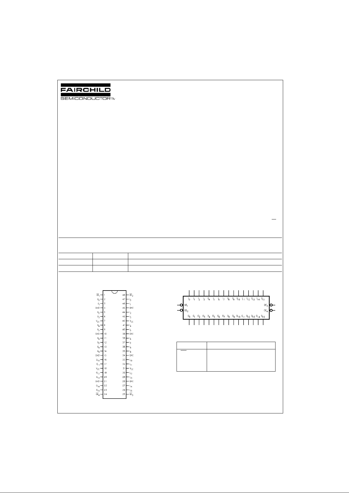
The LCX16244 contain s sixteen n on-inverting b uffers with
3-STATE outputs desig ned to be employed as a memory
and address driver, clock driver, or bus oriented transmitter/receiver. The device is nibble controll ed. Each nibble
has separate 3-STATE control inputs which can be shorted
together for full 16-bit operation.
The LCX16244 is desi gned for low vol tage (2.5V or 3.3V )
V
CC
applications with capability of interfacing to a 5V signal
environment.
The LCX16244 is fabricated with an advanced CMOS tech-
nology to achieve high spee d operation while mai ntaining
CMOS low power dissipation.
Features
■ 5V tolerant inputs and outputs
■ 2.3V–3.6V V
CC
specifications provided
■ 4.5 ns t
PD
max (VCC = 3.0V), 20 µA ICC max
■ Power down high impedance inputs and outputs
■ Supports live insertion/withdrawal (Note 1)
■ ±24 mA output drive (V
CC
= 3.0V)
■ Implements patented noise/EMI reduction circuitry
■ Latch-up performance exceeds 500 mA
■ ESD performance:
Human body model > 2000V
Machine model > 200V
Note 1: To ensure the high-impedance state d uring pow er up or d own OE
should be tied to VCC through a pull-up res istor: the m inimu m value or t he
resistor is determin ed by the current-sourcing capability of the driver.
Ordering Code:
Devices also availab le in Tape and Reel. Specify by appending th e s uffix let t er “X” to the ordering code.
Connection Diagram Logic Symbol
Pin Descriptions
Order Number Package Number Package Description
74LCX16244MEA MS48A 48-Lead Small Shrink Outline Package (SSOP), JEDEC MO-118, 0.300” Wide
74LCX16244MTD MTD48 48-Lead Thin Shrink Small Outline Package (TSSOP), JEDEC MO-153, 6.1mm Wide
Pin Names Description
OE
n
Output Enable Input (Active LOW)
I
0–I15
Inputs
O
0–O15
Outputs
www.fairchildsemi.com 2
74LCX16244
Truth Tables
H = HIGH Voltage Level
L = LOW Voltage Level
X = Immaterial
Z = High Impedance
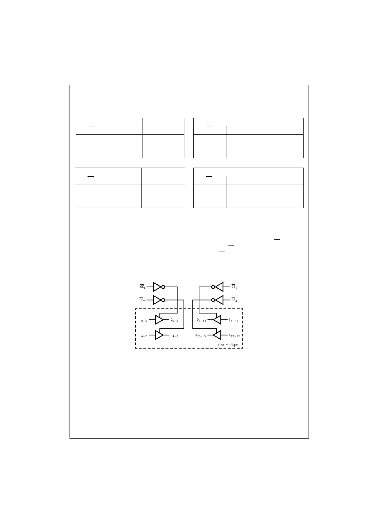
Functional Description
The LCX16244 con tains sixteen non-inverting buffers with
3-STATE standard outputs. The device is nibble (4 bits)
controlled with each nib bl e f unct ioni n g ide ntica l ly, but independent of the other. The control pins can be shorted
together to obtain full 16-bit operation. The 3-STATE out-
puts are controlle d by an Output Enable (OE
n
) input for
each nibble. When OE
n
is LOW, the outputs are in 2-state
mode. When OE
n
is HIGH, the outputs are in the high
impedance mode, but this does not interfere with enteri ng
new data into the inputs.
Logic Diagram
Inputs Outputs
OE
1
I0–I
3
O0–O
3
LL L
LH H
HX Z
Inputs Outputs
OE
3
I8–I
11
O8–O
11
LL L
LH H
HX Z
Inputs Outputs
OE
2
I4–I
7
O4–O
7
LL L
LH H
HX Z
Inputs Outputs
OE
4
I12–I
15
O12–O
15
LL L
LH H
HX Z
3 www.fairchildsemi.com
74LCX16244
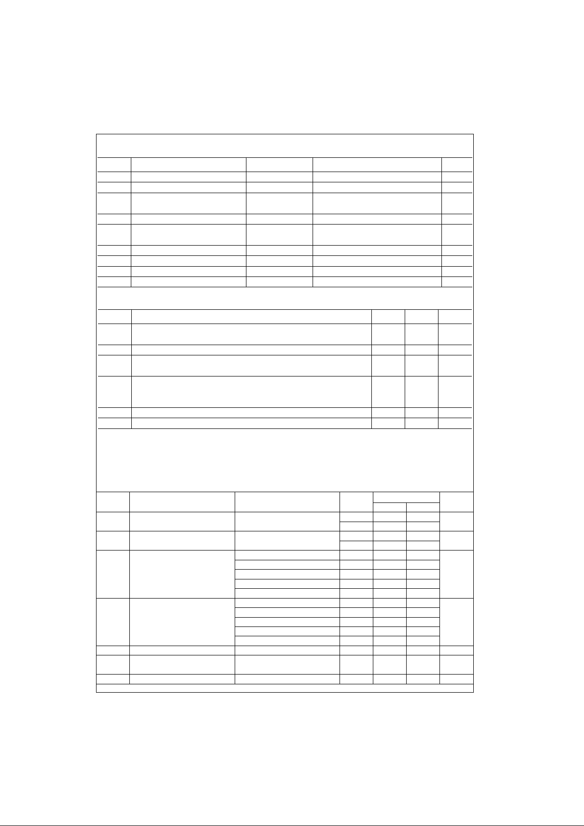
Absolute Maximum Ratings(Note 2)
Recommended Operating Conditions (Note 4)
Note 2: The Absolute Maximum Ratings are those values beyond which the safety of the device cannot be guaranteed. The device should not be operated
at these limits. The parametric values defined in the Electrical Characteristics tables are not guaranteed at the Absolute Maximum Ratings. The “Recommended Operating C onditions” table will def ine the conditions for ac t ual device operation.
Note 3: I
O
Absolute Maximum Rating must be observed.
Note 4: Unused inputs must be held HIGH or LOW. They may not float.
DC Electrical Characteristics
Symbol Parameter Value Conditions Units
V
CC
Supply Voltage −0.5 to +7.0 V
V
I
DC Input Voltage −0.5 to +7.0 V
V
O
DC Output Voltage −0.5 to +7.0 Output in 3-STATE
V
−0.5 to V
CC
+ 0.5 Output in HIGH or LOW State (Note 3)
I
IK
DC Input Diode Current −50 VI < GND mA
I
OK
DC Output Diode Current −50 VO < GND
mA
+50 V
O
> V
CC
I
O
DC Output Source/Sink Current ±50 mA
I
CC
DC Supply Current per Supply Pin ±100 mA
I
GND
DC Ground Current per Ground Pin ±100 mA
T
STG
Storage Temperature −65 to +150 °C
Symbol Parameter Min Max Units
V
CC
Supply Voltage Operating 2.0 3.6
V
Data Retention 1.5 3.6
V
I
Input Voltage 05.5V
V
O
Output Voltage HIGH or LOW State 0 V
CC
V
3-STATE 0 5.5
I
OH/IOL
Output Current VCC = 3.0V − 3.6V ±24
mAV
CC
= 2.7V − 3.0V ±12
V
CC
= 2.3V − 2.7V ±8
T
A
Free-Air Operating Temperature −40 85 °C
∆t/∆V Input Edge Rate, V
IN
= 0.8V–2.0V, VCC = 3.0V 0 10 ns/V
Symbol Parameter Conditions
V
CC
TA = −40°C to +85°C
Units
(V) Min Max
V
IH
HIGH Level Input Voltage 2.3 − 2.7 1.7
V
2.7 − 3.6 2.0
V
IL
LOW Level Input Voltage 2.3 − 2.7 0.7
V
2.7 − 3.6 0.8
V
OH
HIGH Level Output Voltage IOH = −100 µA2.3 − 3.6 VCC − 0.2
V
IOH = −8 mA 2.3 1.8
IOH = −12 mA 2.7 2.2
IOH = −18 mA 3.0 2.4
IOH = −24 mA 3.0 2.2
V
OL
LOW Level Output Voltage IOL = 100 µA2.3 − 3.6 0.2
V
IOL = 8 mA 2.3 0.6
IOL = 12 mA 2.7 0.4
IOL = 16 mA 3.0 0.4
IOL = 24 mA 3.0 0.55
I
I
Input Leakage Current 0 ≤ VI ≤ 5.5V 2.3 − 3.6 ±5.0 µA
I
OZ
3-STATE Output Leakage 0 ≤ VO ≤ 5.5V 2.3 − 3.6 ±5.0
µA
VI = VIH or V
IL
I
OFF
Power-Off Leakage Current VI or VO = 5.5V 0 10 µA
 Loading...