

Fairchild Semiconductor 74LCX16240MTDX, 74LCX16240MTD, 74LCX16240MEAX, 74LCX16240MEA, 74LCX16240CW Datasheet
February 1994
Revised April 1999
74LCX16240 Low Voltage 16-Bit Inverting Buffer/Line Driver with 5V Tolerant Inputs/Outputs
© 1999 Fairchild Semiconductor Corporation DS011999.prf www.fairchildsemi.com
74LCX16240
Low Voltage 16-Bit Inverting Buffer/Line Driver with
5V Tolerant Inputs/Outputs
General Description
The LCX16240 contains sixteen inverting buffers with 3STATE outputs designed to be employed as a memory and
address driver, clock driver, or bus-oriented transmitter/
receiver. The device is nibble controlled. Each nibble has
separate 3-STATE control inputs which can be shorted
together for full 16-bit operation.
The LCX16240 is desi gned for low vol tage (2.5V or 3.3V )
V
CC
applications with capacity o f inter facin g to a 5V signal
environment.
The LCX16240 is fabricated with an advanced CMOS tech-
nology to achieve high spee d operation while mai ntaining
CMOS low power dissipation.
Features
■ 5V tolerant inputs and outputs
■ 2.3V–3.6V V
CC
specifications provided
■ 4.5 ns t
PD
max (VCC = 3.3V), 20 µA ICC max
■ Power down high impedance inputs and outputs
■ Supports live insertion/withdrawal (Note 1)
■ ±24 mA output drive (V
CC
= 3.0V)
■ Implements patented noise/EMI reduction circuitry
■ Latch-up performance exceeds 500 mA
■ ESD performance:
Human body model > 2000V
Machine model > 200V
Note 1: To ensure the high-impedan c e state during power up or down, OE
should be tied to V
CC
through a pull-up re sistor: the minim um val ue or the
resistor is determin ed by the current-sourcin g c apability of the driver.
Ordering Code:
Devices also availab le in Tape and Reel. Specify by appending th e s uffix let t er “X” to the ordering code.
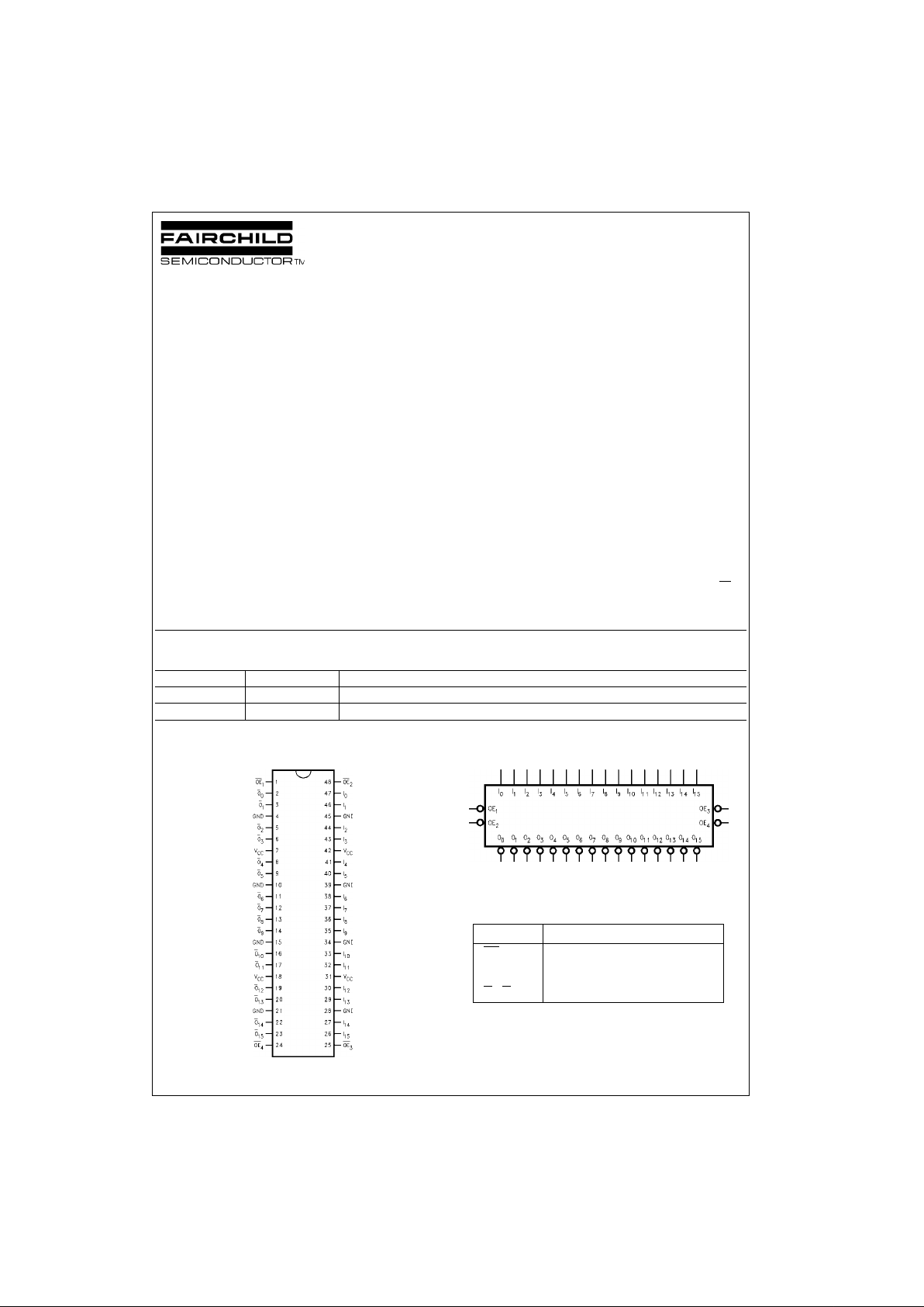
Connection Diagram Logic Symbol
Pin Descriptions
Order Number Package Number Package Description
74LCX16240MEA MS48A 48-Lead Small Shrink Outline Package (SSOP), JEDEC MO-118, 0.300” Wide
74LCX16240MTD MTD48 48-Lead Thin Shrink Small Outline Package (TSSOP), JEDEC MO-153, 6.1mm Wide
Pin Names Description
OE
n
Output Enable Inputs (Active LOW)
I
0–I15
Inputs
O
0–O15
Outputs
www.fairchildsemi.com 2
74LCX16240
Truth Tables
H = HIGH Voltage Level
L = LOW Voltage Level
X = Immaterial
Z = High Impedance
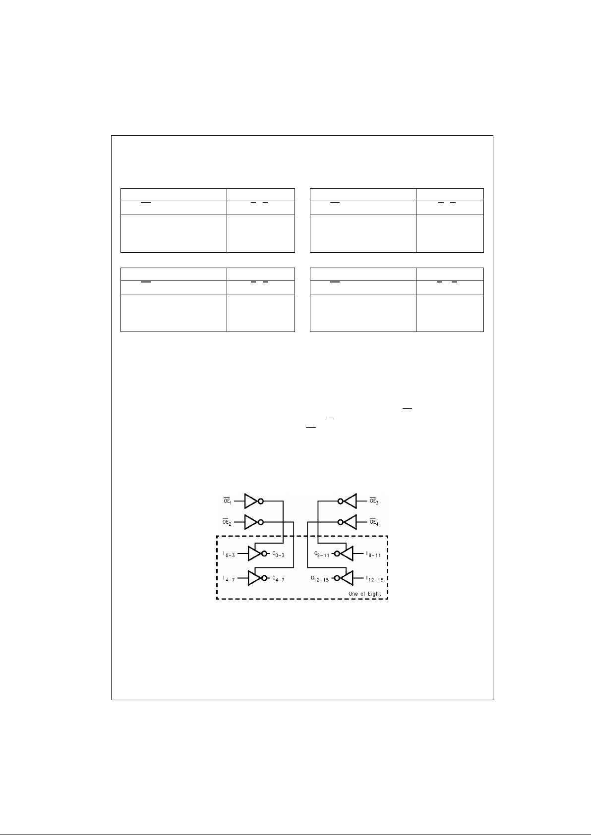
Functional Description
The LCX16240 contains si xteen inverting buffers with 3STATE standard outputs. The de vice is n ibble (4 bits) controlled with each nibble fun cti on ing ide nti ca lly, but independent of the other. The control pins may be shorted together
to obtain full 16-bit operation. The 3-STATE outputs are
controlled by an Output Enable (OEn) input for each nibble.
When OE
n
is LOW, the outputs are in 2- stat e m od e. Wh en
OE
n
is HIGH, the outputs are in the high impedance mode,
but this does not inte rfere with enteri ng new data into the
inputs.
Logic Diagram
Inputs Outputs
OE
1
I0–I
3
O0–O
3
LL H
LH L
HX Z
Inputs Outputs
OE
3
I8–I
11
O8–O
11
LL H
LH L
HX Z
Inputs Outputs
OE
2
I4–I
7
O4–O
7
LL H
LH L
HX Z
Inputs Outputs
OE
4
I12–I
15
O12–O
15
LL H
LH L
HX Z
3 www.fairchildsemi.com
74LCX16240
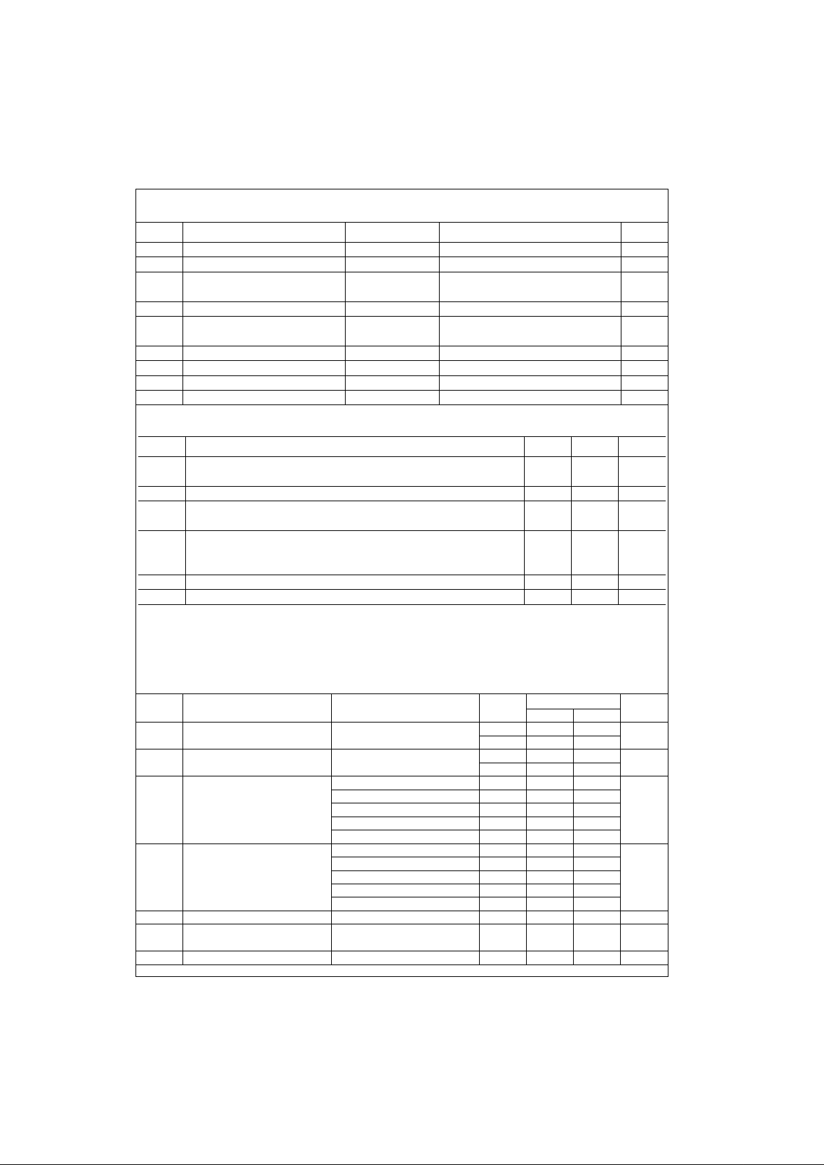
Absolute Maximum Ratings(Note 2)
Recommended Operating Conditions (Note 4)
Note 2: The Absolute Maximum Ratings are those values beyond which the safety of the device cannot be guaranteed. The device should not be operated
at these limits. The parametric values defined in the Electrical Characteristics tables are not guaranteed at the Absolute Maximum Ratings. The “Recommended Operating C onditions” table will define the conditions for actual device operation.
Note 3: I
O
Absolute Maximum Rating must be observed.
Note 4: Unused inputs must be held HIGH or LOW. They may not float.
DC Electrical Characteristics
Symbol Parameter Value Conditions Units
V
CC
Supply Voltage −0.5 to +7.0 V
V
I
DC Input Voltage −0.5 to +7.0 V
V
O
DC Output Voltage −0.5 to +7.0 Output in 3-STATE
V
−0.5 to V
CC
+ 0.5 Output in HIGH or LOW State (Note 3)
I
IK
DC Input Diode Current −50 VI < GND mA
I
OK
DC Output Diode Current −50 VO < GND
mA
+50 V
O
> V
CC
I
O
DC Output Source/Sink Current ±50 mA
I
CC
DC Supply Current per Supply Pin ±100 mA
I
GND
DC Ground Current per Ground Pin ±100 mA
T
STG
Storage Temperature −65 to +150 °C
Symbol Parameter Min Max Units
V
CC
Supply Voltage Operating 2.0 3.6
V
Data Retention 1.5 3.6
V
I
Input Voltage 05.5V
V
O
Output Voltage HIGH or LOW State 0 V
CC
V
3-STATE 0 5.5
I
OH/IOL
Output Current VCC = 3.0V − 3.6V ±24
mAV
CC
= 2.7V − 3.0V ±12
V
CC
= 2.3V − 2.7V ±8
T
A
Free-Air Operating Temperature −40 85 °C
∆t/∆V Input Edge Rate, V
IN
= 0.8V–2.0V, VCC = 3.0V 0 10 ns/V
Symbol Parameter Conditions
V
CC
TA = −40°C to +85°C
Units
(V) Min Max
V
IH
HIGH Level Input Voltage 2.3 − 2.7 1.7
V
2.7 − 3.6 2.0
V
IL
LOW Level Input Voltage 2.3 − 2.7 0.7
V
2.7 − 3.6 0.8
V
OH
HIGH Level Output Voltage IOH = −100 µA2.3 − 3.6 VCC − 0.2
V
IOH = −8 mA 2.3 1.8
IOH = −12 mA 2.7 2.2
IOH = −18 mA 3.0 2.4
IOH = −24 mA 3.0 2.2
V
OL
LOW Level Output Voltage IOL = 100 µA2.3 − 3.6 0.2
V
IOL = 8 mA 2.3 0.6
IOL = 12 mA 2.7 0.4
IOL = 16 mA 3.0 0.4
IOL = 24 mA 3.0 0.55
I
I
Input Leakage Current 0 ≤ VI ≤ 5.5V 2.3 − 3.6 ±5.0 µA
I
OZ
3-STATE Output Leakage 0 ≤ VO ≤ 5.5V 2.3 − 3.6 ±5.0
µA
VI = VIH or V
IL
I
OFF
Power-Off Leakage Current VI or VO = 5.5V 0 10 µA
 Loading...