

Fairchild Semiconductor 74LCX14SJ, 74LCX14MX, 74LCX14MTCX, 74LCX14MTC, 74LCX14M Datasheet
...
March 1995
Revised March 1999
74LCX14 Low Voltage Hex Inverter with 5V Tolerant Schmitt Trigger Inputs
© 1999 Fairchild Semiconductor Corporation DS012412.prf www.fairchildsemi.com
74LCX14
Low Voltage Hex Inverter
with 5V Tolerant Schmitt Trigger Inputs
General Description
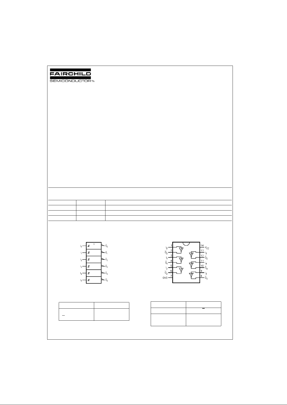
The LCX14 contains six inverter gat es each with a Schmitt
trigger input. They are capable of transforming slowly
changing input signals in to sharply defined, jitte r-free output signals. In additio n, they have a greater no ise margin
than conventional inverters.
The LCX14 has hysteresis b etween th e positi ve-go ing and
negative-going input thresholds (typically 1.0V) which is
determined internall y by transistor ratios an d is essentially
insensitive to temperature and supply voltage variations.
The inputs tolerate voltages up to 7V allowing the interface
of 5V, 3V and 2.5V systems.
The 74LCX14 is fabricated with advanced CMO S technology to achieve high speed operation while maintaining
CMOS low power dissipation.
Features
■ 5V tolerant inputs
■ 2.3V–3.6V V
CC
specifications provided
■ 6.5 ns t
PD
max (V
CC
= 3.3V), 10 µA ICC max
■ Power down high impedance inputs and outputs
■ ±24 mA output drive (V
CC
= 3.0V)
■ Implements patented noise/EMI reduction circuitry
■ Latch-up performance exceeds 500 mA
■ ESD performance:
Machine model > 2000V
Human model > 200V
Ordering Code:
Devices also availab le in Tape and Reel. Specify by appending th e s uffix let t er “X” to the ordering code.
Logic Symbol
IEEE/IEC
Pin Descriptions
Connection Diagram
Truth Table
Order Number Package Number Package Description
74LCX14M M14A 14-Lead Small Outline Integrated Circuit (SOIC), JEDEC MS-120, 0.150” Narrow
74LCX14SJ M14D 14-Lead Small Outline Package (SOP), EIAJ TYPE II, 5.3mm Wide
74LCX14MTC MTC14 14-Lead Thin Shrink Small Outline Package (TSSOP), JEDEC MO-153, 4.4mm Wide
Pin Names Description
I
n
Inputs
O
n
Outputs
Input Output
AO
L H
H L
www.fairchildsemi.com 2
74LCX14
Absolute Maximum Ratings(Note 1)
Recommended Operating Conditions (Note 3)
Note 1: The Absolute Maximum Ratings are those values beyond which the safety of the device cannot be guaranteed. The device should not be operated
at these limits. Th e parametric values def ined in the Electrical Cha racteristic s tables are not guaran teed at the A bsolute Ma ximum Rating s. The “Rec ommended Operat ing Conditions” table will define the conditions fo r ac t ual device operation.
Note 2: I
O
Absolute Maximum Rating must be observed.
Note 3: Unused inputs must be held HIGH or LOW. They may not float.
DC Electrical Characteristics
Symbol Parameter Value Conditions Units
V
CC
Supply Voltage −0.5 to +7.0 V
V
I
DC Input Voltage −0.5 to +7.0 V
V
O
DC Output Voltage −0.5 to VCC + 0.5 Output in HIGH or LOW State (Note 2) V
I
IK
DC Input Diode Current −50 VI < GND mA
I
OK
DC Output Diode Current −50 VO < GND
mA
+50 V
O
> V
CC
I
O
DC Output Source/Sink Current ±50 mA
I
CC
DC Supply Current per Supply Pin ±100 mA
I
GND
DC Ground Cu rrent per Ground Pin ±100 mA
T
STG
Storage Temperature −65 to +150 °C
Symbol Parameter Min Max Units
V
CC
Supply Voltage Operating 2 .0 3.6
V
Data Retention 1.5 3.6
V
I
Input Voltage 05.5V
V
O
Output Voltage HIGH or LOW State 0 V
CC
V
I
OH/IOL
Output Current VCC = 3.0V − 3.6V ±24
mAV
CC
= 2.7V − 3.0V ±12
V
CC
= 2.3V − 2.7V ±8
Symbol Parameter Conditions
V
CC
TA = −40°C to +85°C
Units
(V) Min Max
V
t+
Positive Input Threshold 2.5 0.9 1.7
V
3.0 1.2 2.2
V
t−
Negative Input Threshold 2.5 0.4 1.1
V
3.0 0.6 1.5
V
H
Hysteresis 2.5 0.3 1.0
V
3.0 0.4 1.2
V
OH
HIGH Level Output Voltage IOH = −100µA2.3 − 3.6 VCC - 0.2
V
IOH = -8 mA 2.3 1.8
IOH = −12 mA 2.7 2.2
IOH = −18 mA 3.0 2.4
IOH = −24 mA 3.0 2.2
V
OL
LOW Level Output Voltage IOL = 100µA2.3 − 3.6 0.2
V
IOL = 8mA 2.3 0.6
IOL = 12 mA 2.7 0.4
IOL = 16 mA 3.0 0.4
IOL = 24 mA 3.0 0.55
I
I
Input Leakage Current 0 ≤ VI ≤ 5.5V 2.3 − 3.6 ±5.0 µA
I
OFF
Power-Off Leakage Current VI or VO = 5.5V 0 10 µA
I
CC
Quiescent Supply Current VI = VCC or GND 2.3 − 3.6 10
µA
3.6V ≤ VI ≤ 5.5V 2.3 − 3.6 ±10
∆I
CC
Increase in ICC per Input VIH = VCC −0.6V 2.3 − 3.6 500 µA
3 www.fairchildsemi.com
74LCX14
AC Electrical Characteristics
Note 4: Skew is def ined as the absolut e v alue of the difference between the actual propagation delay f or any two separate outputs of the same device. The
specification applies t o any outputs switching in th e s am e direction, either HIG H -t o-LOW (t
OSHL
) or LOW-to-HIGH (t
OSLH
).
Dynamic Switching Characteristics
Capacitance
Symbol Parameter
TA = −40°C to +85°C, RL = 500 Ω
Units
VCC = 3.3V ± 0.3V VCC = 2.7V VCC = 2.5V ± 0.2V
CL= 50 pF CL = 50 pF CL = 30 pF
Min Max Min Max Min Max
t
PHL
Propagation Delay Time 1.5 6.5 1.5 7.5 1.5 7.8
ns
t
PLH
1.5 6.5 1.5 7.5 1.5 7.8
t
OSHL
Output to Output Skew 1.0
ns
t
OSLH
(Note 4) 1.0
Symbol Parameter Conditions
V
CC
(V)
TA = 25°C
Units
Typical
V
OLP
Quiet Output Dynamic Peak V
OL
CL = 50 pF, VIH =3.3V, VIL = 0V 3.3 0.8
V
CL = 30 pF, VIH = 2.5V, VIL = 0V 2.5 0.6
V
OLV
Quiet Output Dynamic Valley V
OL
CL = 50 pF, VIH = 3.3V, VIL = 0V 3.3 −0.8
V
CL = 30 pF, VIH =2.5V, VIL = 0V 2.5 −0.6
Symbol Parameter Conditions Typical Units
C
IN
Input Capacitance VCC = Open, VI = 0V or V
CC
7pF
C
OUT
Output Capacitance VCC = 3.3V, VI = 0V or V
CC
8pF
C
PD
Power Dissipation Capacitance VCC = 3.3V, VI = 0V or VCC, f = 10 MHz 25 pF
 Loading...