

Fairchild Semiconductor 74LCX138CW, 74LCX138SJX, 74LCX138SJ, 74LCX138MX, 74LCX138MTCX Datasheet
...
March 1995
Revised March 1999
74LCX138 Low Voltage 1-of-8 Decoder/Demultiplexer with 5V Tolerant Inputs
© 1999 Fairchild Semiconductor Corporation DS012417.prf www.fairchildsemi.com
74LCX138
Low Voltage 1-of-8 Decoder/Demultiplexer
with 5V Tolerant Inputs
General Description
The LCX138 is a hi g h- spee d 1- of-8 decoder/demultipl ex er.
This device is ideally suited for high-speed memory chip
select address decoding . The multip le input enables allow
parallel expansion to a 1-of-24 decoder using just three
LCX138 devices or a 1-of-32 decoder u sing four LCX138
devices and one inverter.
The 74LCX138 is fabricated with advanced CMOS technology to achieve high speed operation while maintaining
CMOS low power dissipation.
Features
■ 5V tolerant inputs
■ 2.3V–3.6V V
CC
specifications provided
■ 6.0 ns t
PD
max (VCC = 3.3V), 10 µA ICC max
■ Power down high impedance inputs and outputs
■ ±24 mA output drive (V
CC
= 3.0V)
■ Implements patented noise/EMI reduction circuitry
■ Latch-up performance exceeds 500 mA
■ ESD performance:
Human body model > 2000V
Machine model > 200V
Ordering Code:
Devices also availab le in Tape and R eel. Specify by appending suffix letter “X” to the ordering code.
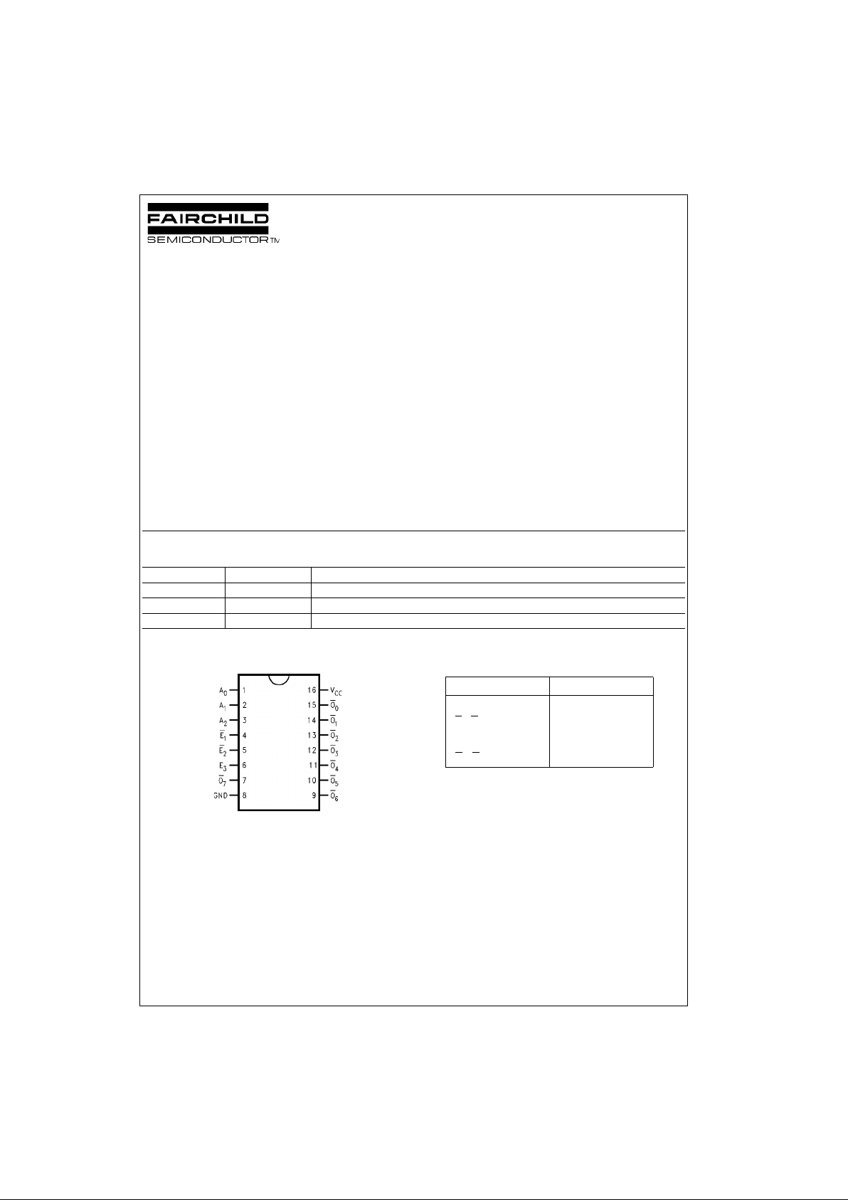
Connection Diagram Pin Descriptions
Order Number Package Number Package Description
74LCX138M M16A 16-Lead Small Outline Integrated Circuit (SOIC), JEDEC MS-012, 0.150” Narrow
74LCX138SJ M16D 16-Lead Small Outline Package (SOP), EIAJ TYPE II, 5.3mm Wide
74LCX138MTC MTC16 16-Lead Thin Shrink Small Outline Package (TSSOP), JEDEC MO-153, 4.4mm Wide
Pin Names Description
A
0–A2
Address Inputs
E
1–E2
Enable Inputs
E
3
Enable Input
O
0–O7
Outputs
www.fairchildsemi.com 2
74LCX138
Functional Description
The LCX138 high-speed 1-of-8 decoder/demultiplexer
accepts three binary weighted inputs (A
0
, A1, A2) and,
when enabled, provides eight mutually exclusive activeLOW outputs (O
0–O7
). The LCX138 fe atures three Enab le
inputs, two active-LOW (E
1
, E2) and one active-HIGH (E3).
All outputs will be HIGH unless E
1
and E2 are LOW and E
3
is HIGH. The LCX138 can b e u sed as an 8-output demulti plexer by using one of the active LOW Enable inputs as the
data input and the other Enable inputs as strobes. The
Enable inputs which are not used must be permanently tied
to their appropriate active-HIGH or active-LOW state.
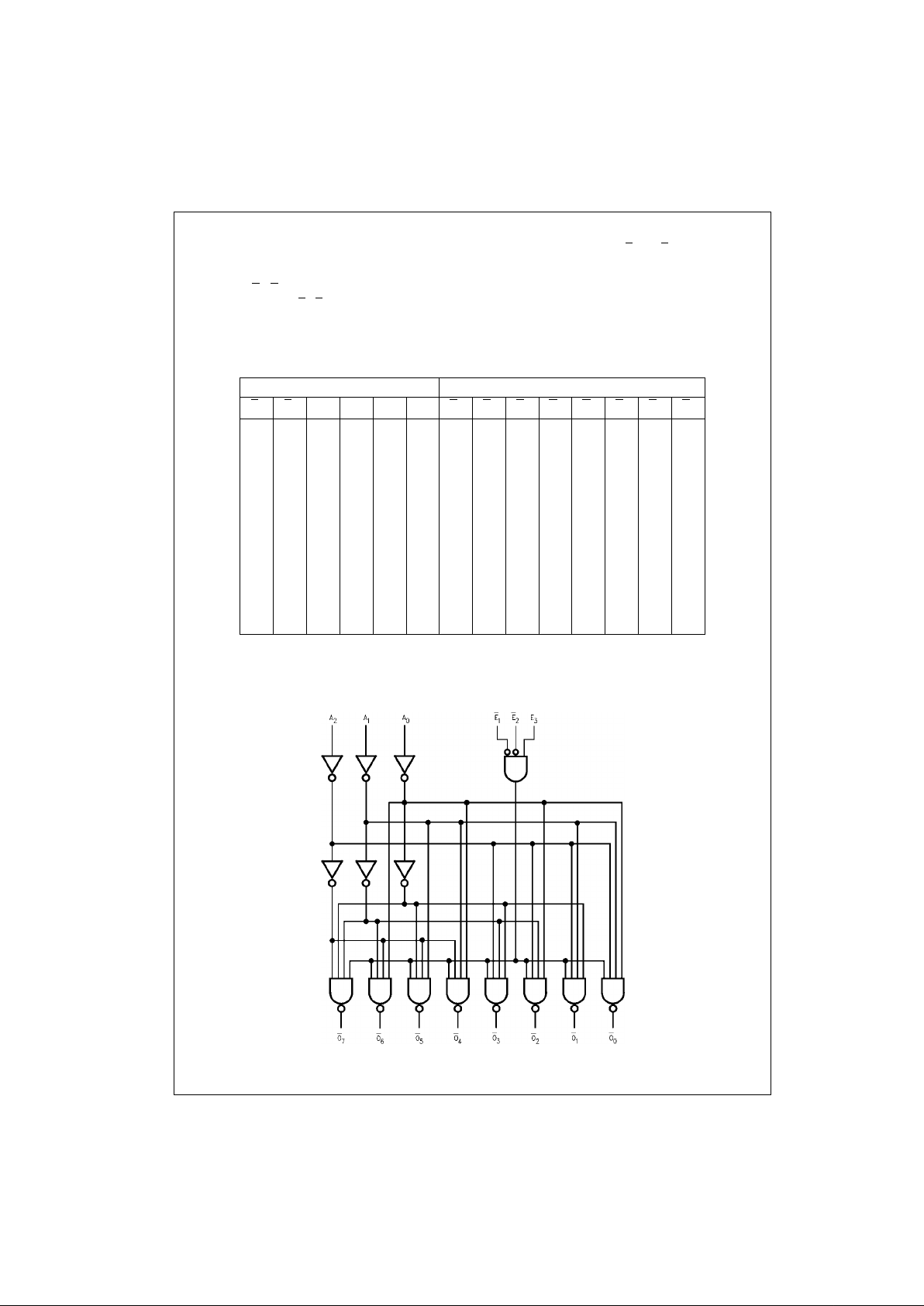
Truth Table
H = HIGH Voltage Level
L = LOW Voltage Level
X = Immaterial
Logic Diagram
Please note that this diagram is provided only f or t he understanding of logic operations and should not be used to estimate propa gation delays.
Inputs Outputs
E
1E2E3A0A1A2O0O1O2O3O4O5O6O7
HXXXXXHHHHHHHH
XHXXXXHHHHHHHH
XXLXXXHHHHHHHH
LLHLLLLHHHHHHH
LLHHLLHLHHHHHH
LLHLHLHHLHHHHH
LLHHHLHHHLHHHH
LLHLLHHHHHLHHH
LLHHLHHHHHHLHH
LLHLHHHHHHHHLH
LLHHHHHHHHHHHL
3 www.fairchildsemi.com
74LCX138
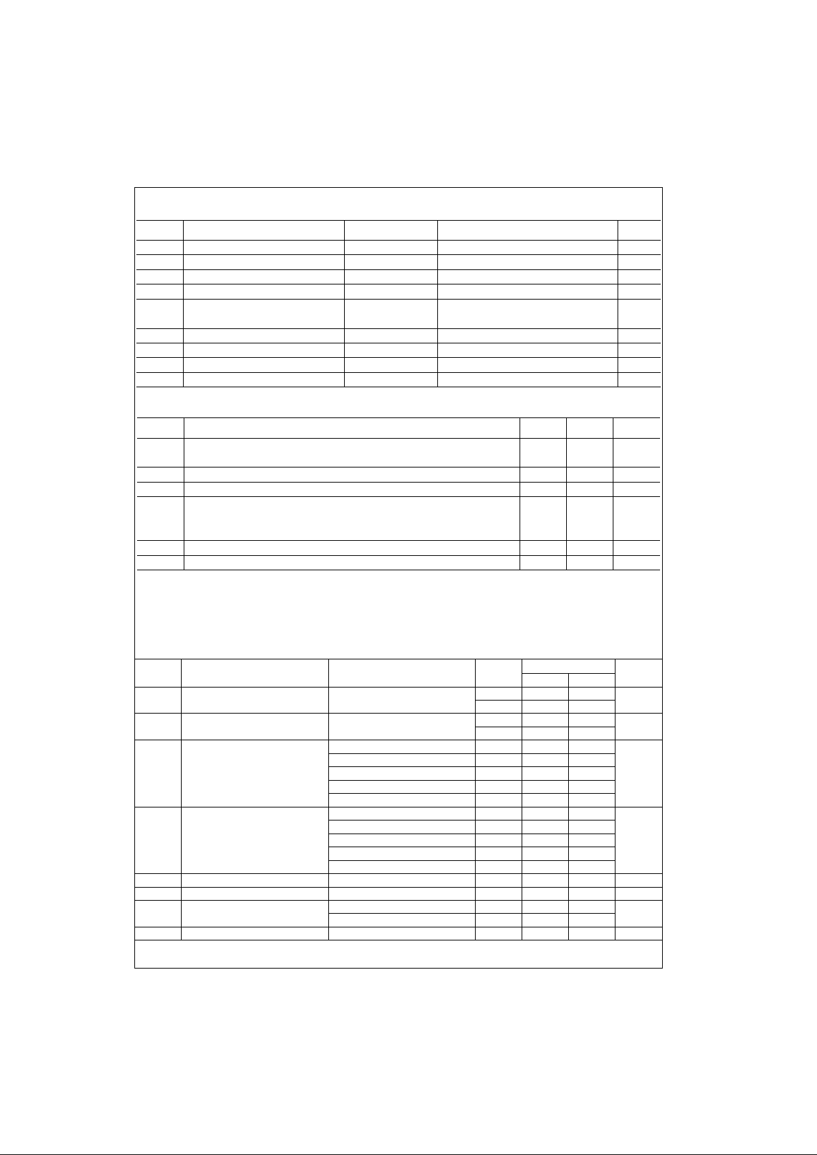
Absolute Maximum Ratings(Note 1)
Recommended Operating Conditions (Note 3)
Note 1: The Absolute Maximum Ratings are those values beyond which the safety of the device cannot be guaranteed. The device should not be operated
at these limits. The parametric values defined in the Electrical Characteristics tables are not guaranteed at the Absolute Maximum Ratings. The “Recommended Operating C onditions” table will define the conditions for actua l dev ic e operation.
Note 2: I
O
Absolute Maximum Rating must be observed.
Note 3: Unused inputs must be held HIGH or LOW. They may not float.
DC Electrical Characteristics
Symbol Parameter Value Conditions Units
V
CC
Supply Voltage −0.5 to +7.0 V
V
I
DC Input Voltage −0.5 to +7.0 V
V
O
DC Output Voltage −0.5 to VCC + 0.5 Output in HIGH or LOW State (Note 2) V
I
IK
DC Input Diode Current −50 VI < GND mA
I
OK
DC Output Diode Current −50 VO < GND
mA
+50 V
O
> V
CC
I
O
DC Output Source/Sink Current ±50 mA
I
CC
DC Supply Current per Supply Pin ±100 mA
I
GND
DC Ground Current per Ground Pin ±100 mA
T
STG
Storage Temperature −65 to +150 °C
Symbol Parameter Min Max Units
V
CC
Supply Voltage Operating 2.0 3.6
V
Data Retention 1.5 3.6
V
I
Input Voltage 05.5V
V
O
Output Voltage HIGH or LOW State 0 V
CC
V
I
OH/IOL
Output Current VCC = 3.0V − 3.6V ±24
mAV
CC
= 2.7V − 3.0V ±12
V
CC
= 2.3V − 2.7V ±8
T
A
Free-Air Operating Temperature −40 85 °C
∆t/∆V Input Edge Rate, V
IN
= 0.8V–2.0V, VCC = 3.0V 0 10 ns/V
Symbol Parameter Conditions
V
CC
TA = −40°C to +85°C
Units
(V) Min Max
V
IH
HIGH Level Input Voltage 2.3 − 2.7 1.7
V
2.7 − 3.6 2.0
V
IL
LOW Level Input Voltage 2.3 − 2.7 0.7
V
2.7 − 3.6 0.8
V
OH
HIGH Level Output Voltage IOH = −100 µA2.3 − 3.6 VCC − 0.2
V
IOH = -8 mA 2.3 1.8
IOH = −12 mA 2.7 2.2
IOH = −18 mA 3.0 2.4
IOH = −24 mA 3.0 2.2
V
OL
LOW Level Output Voltage IOL = 100 µA2.3 − 3.6 0.2
V
IOL = 8mA 2.3 0.6
IOL = 12 mA 2.7 0.4
IOL = 16 mA 3.0 0.4
IOL = 24 mA 3.0 0.55
I
I
Input Leakage Current 0 ≤ VI ≤ 5.5V 2.3 − 3.6 ±5.0 µA
I
OFF
Power-Off Leakage Current VI or VO = 5.5V 0 10 µA
I
CC
Quiescent Supply Current VI = VCC or GND 2.3 − 3.6 10
µA
3.6V ≤ VI ≤ 5.5V 2.3 − 3.6 ±10
∆I
CC
Increase in ICC per Input VIH = VCC −0.6V 2.3 − 3.6 500 µA
 Loading...