

Fairchild Semiconductor 74LCX125M, 74LCX125CW, 74LCX125SJX, 74LCX125SJ, 74LCX125MX Datasheet
...
March 1995
Revised April 1999
74LCX125 Low Voltage Quad Buffer with 5V Tolerant Inputs and Outputs
© 1999 Fairchild Semiconductor Corporation DS012416.prf www.fairchildsemi.com
74LCX125
Low Voltage Quad Buffer
with 5V Tolerant Inputs and Outputs
General Description
The LCX125 conta ins four i ndepend ent non-in verting buffers with 3-STATE outputs. The inputs tolerate voltag es up
to 7V allowing the interface of 5V systems to 3V systems.
The 74LCX125 is fabricated with an advanced CMOS technology to achieve high spee d operation while mai ntaining
CMOS low power dissipation.
Features
■ 5V tolerant inputs and outputs
■ 2.3V–3.6V V
CC
specifications provided
■ 6.0 ns t
PD
max (VCC = 3.3V), 10 µA ICC max
■ Power down high impedance inputs and outputs
■ Supports live insertion/withdrawal (Note 1)
■ ±24 mA output drive (V
CC
= 3.0V)
■ Implements patented noise/EMI reduction circuitry
■ Latch-up performance exceeds 500 mA
■ ESD performance:
Human body model > 2000V
Machine model > 100V
Note 1: To ensure the high-impedan c e state during power up or down, OE
should be tied to VCC through a pull-up res istor: the m inimu m value or t he
resistor is determin ed by the current-sourcing capability of the driv er.
Ordering Code:
Device also available in Tape and Reel. Specify by appending s uffix let te r “X” to the ordering code .
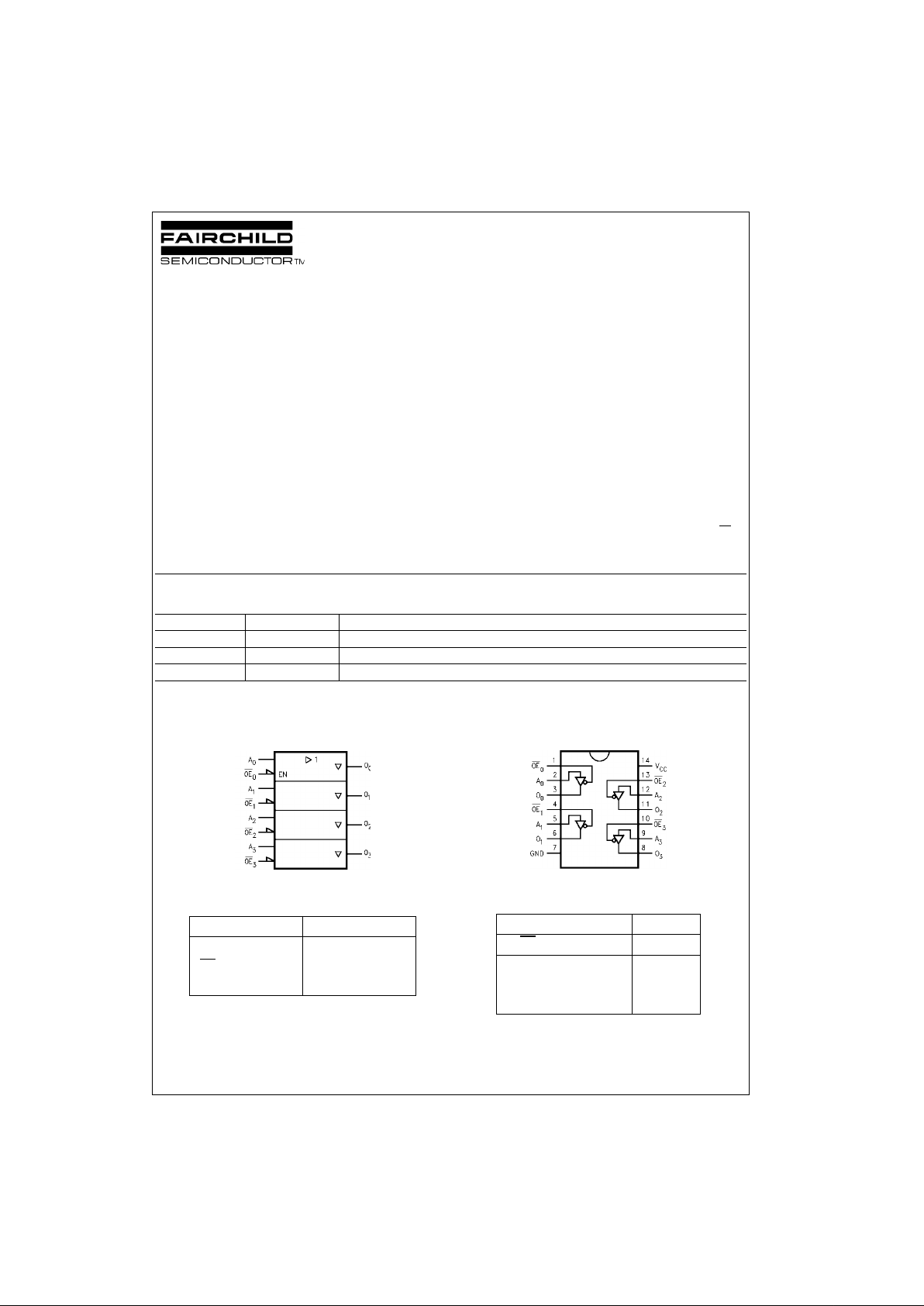
Logic Symbol
IEEE/IEC
Pin Descriptions
Connection Diagram
Truth Table
H = HIGH Voltage Level
L = LOW Voltage Level
Z = High Impedance
X = Immaterial
Order Number Package Number Package Description
74LCX125M M14A 14-Lead Small Outline Integrated Circuit (SOIC), JEDEC MS-120, 0.150” Narrow
74LCX125SJ M14D 14-Lead Small Outline Package (SOP), EIAJ TYPE II, 5.3mm Wide
74LCX125MTC MTC14 14-Lead Thin Shrink Small Outline Package (TSSOP), JEDEC MO-153, 4.4mm Wide
Pin Names Description
A
n
Inputs
OE
n
Output Enable Inputs
O
n
Outputs
Inputs Output
OE
n
A
n
O
n
LLL
LHH
HXZ
www.fairchildsemi.com 2
74LCX125
Absolute Maximum Ratings(Note 2)
Recommended Operating Conditions (Note 4)
Note 2: The Absolute Maximum Ratings are those values beyond which the safety of the device cannot be guaranteed. The device should not be operated
at these limits. Th e parametric values def ined in the Electrical Cha racteristic s tables are not guaran teed at the A bsolute Ma ximum Rating s. The “Rec ommended Operat ing Conditions” table w ill define the conditions fo r ac t ual device operation.
Note 3: I
O
Absolute Maximum Rating must be observed.
Note 4: Unused inputs or I/Os must be held HIGH or LOW. They may not float.
DC Electrical Characteristics
Symbol Parameter Value Conditions Units
V
CC
Supply Voltage −0.5 to +7.0 V
V
I
DC Input Voltage −0.5 to +7.0 V
V
O
DC Output Voltage −0.5 to +7.0 Output in 3-STATE V
−0.5 to V
CC
+ 0.5 Output in HIGH or LOW State (Note 3) V
I
IK
DC Input Diode Current −50 VI < GND mA
I
OK
DC Output Diode Current −50 VO < GND
mA
+50 V
O
> V
CC
I
O
DC Output Source/Sink Current ±50 mA
I
CC
DC Supply Current per Supply Pin ±100 mA
I
GND
DC Ground Cu rrent per Ground Pin ±100 mA
T
STG
Storage Temperature −65 to +150 °C
Symbol Parameter Min Max Units
V
CC
Supply Voltage Operating 2 .0 3.6 V
Data Retention 1.5 3.6
V
I
Input Voltage 05.5V
V
O
Output Voltage HIGH or LOW State 0 V
CC
V
3-STATE 0 5.5
I
OH/IOL
Output Current VCC = 3.0V − 3.6V ±24
mAV
CC
= 2.7V − 3.0V ±12
V
CC
= 2.3V − 2.7V ±8
T
A
Free-Air Operating Temperature −40 85 °C
∆t/∆V Input Edge Rate, V
IN
= 0.8V–2.0V, VCC = 3.0V 0 10 ns/V
Symbol Parameter Conditions
V
CC
TA = −40°C to +85°C
Units
(V) Min Max
V
IH
HIGH Level Input Voltage 2.3 − 2.7 1.7
V
2.7 − 3.6 2.0
V
IL
LOW Level Input Voltage 2.3 − 2.7 0.7
V
2.7 − 3.6 0.8
V
OH
HIGH Level Output Voltage IOH = −100 µA2.3 − 3.6 VCC − 0.2
V
IOH = -8 mA 2.3 1.8
IOH = −12 mA 2.7 2.2
IOH = −18 mA 3.0 2.4
IOH = −24 mA 3.0 2.2
V
OL
LOW Level Output Voltage IOL = 100 µA2.3 − 3.6 0.2
V
IOL = 8mA 2.3 0.6
IOL = 12 mA 2.7 0.4
IOL = 16 mA 3.0 0.4
IOL = 24 mA 3.0 0.55
I
I
Input Leakage Current 0 ≤ VI ≤ 5.5V 2.3 − 3.6 ±5.0 µA
I
OZ
3-STATE Output Leakage 0 ≤ VO ≤ 5.5V 2.3 − 3.6 ±5.0 µA
VI = VIH or V
IL
I
OFF
Power-Off Leakage Current VI or VO = 5.5V 0 10 µA
3 www.fairchildsemi.com
74LCX125
DC Electrical Characteristics (Continued)
Note 5: Outputs disab led or 3-STATE only.
AC Electrical Characteristics
Note 6: Skew is def ined as the absol ut e v alue of the difference between the actu al propagation delay f or any two separat e outputs of the same device. The
specification applies t o any outputs switching in the same direction, ei th er HIGH-to-LOW (t
OSHL
) or LOW-to-HIGH (t
OSLH
).
Dynamic Switching Characteristics
Capacitance
Symbol Parameter Conditions
V
CC
TA = −40°C to +85°C
Units
(V) Min Max
I
CC
Quiescent Supply Current VI = VCC or GND 2.3 − 3.6 10
µA
3.6V ≤ VI, VO ≤ 5.5V (Note 5) 2.3 − 3.6 ±10
∆I
CC
Increase in ICC per Input VIH = VCC −0.6V 2.3 − 3.6 500 µA
Symbol Parameter
TA = −40°C to +85°C, RL = 500Ω
Units
VCC = 3.3V ± 0.3V VCC = 2.7V VCC = 2.5V ± 0.2V
CL = 50 pF CL = 50 pF CL = 30 pF
Min Max Min Max Min Max
t
PHL
Propagation Delay 1.5 6.0 1.5 6.5 1.5 7.2
ns
t
PLH
1.5 6.0 1.5 6.5 1.5 7.2
t
PZL
Output Enable Time 1.5 7.0 1.5 8.0 1.5 9.1
ns
t
PZH
1.5 7.0 1.5 8.0 1.5 9.1
t
PLZ
Output Disable Time 1.5 6.0 1.5 7.0 1.5 7.2
ns
t
PHZ
1.5 6.0 1.5 7.0 1.5 7.2
t
OSHL
Output to Output Skew (Note 6) 1.0
ns
t
OSLH
1.0
Symbol Parameter Conditions
V
CC
(V)
TA = 25°C
Units
Typical
V
OLP
Quiet Output Dynamic Peak V
OL
CL = 50 pF, VIH = 3.3V, VIL = 0V 3.3 0.8
V
CL = 30 pF, VIH = 2.5V, VIL = 0V 2.5 0.6
V
OLV
Quiet Output Dynamic Valley V
OL
CL = 50 pF, VIH = 3.3V, VIL = 0V 3.3 −0.8
V
CL = 30 pF, VIH = 2.5V, VIL = 0V 2.5 −0.6
Symbol Parameter Conditions Typical Units
C
IN
Input Capacitance VCC = Open, VI = 0V or V
CC
7pF
C
OUT
Output Capacitance VCC = 3.3V, VI = 0V or V
CC
8pF
C
PD
Power Dissipation Capacitance VCC = 3.3V, VI = 0V or VCC, f = 10 MHz 25 pF
 Loading...