

Fairchild Semiconductor 74LCX04CW, 74LCX04SJX, 74LCX04SJ, 74LCX04MX, 74LCX04MTCX Datasheet
...
March 1995
Revised May 1999
74LCX04 Low Voltage Hex Inverter with 5V Tolerant Inputs
© 1999 Fairchild Semiconductor Corporation DS012410.prf www.fairchildsemi.com
74LCX04
Low Voltage Hex Inverter with 5V Tolerant Inputs
General Description
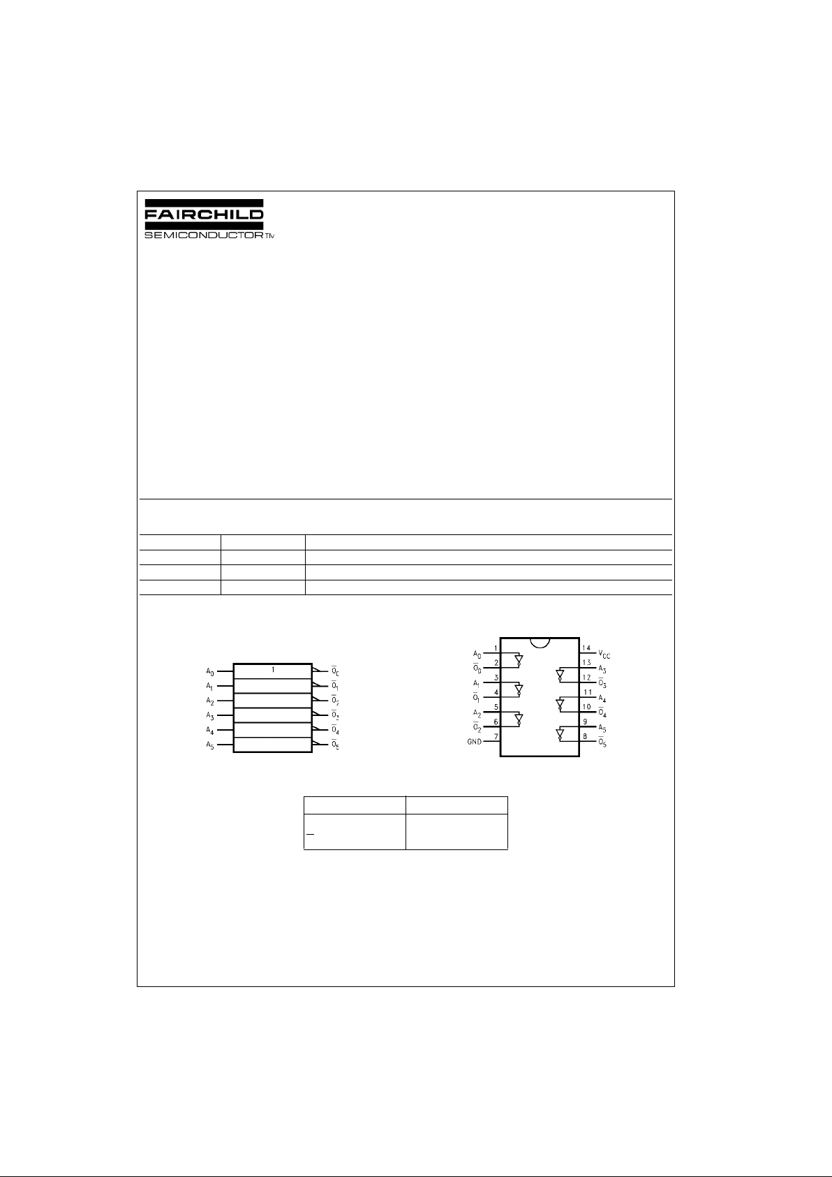
The LCX04 contains six in verters. The i nputs toler ate voltages up to 7V allowing the interface of 5V systems to 3V
systems.
The 74LCX04 is fabricated with advanced CMO S technology to achieve high speed operation while maintaining
CMOS low power dissipation.
Features
■ 5V tolerant inputs
■ 2.3V–3.6V V
CC
specifications provided
■ 5.2 ns t
PD
max (V
CC
= 3.3V), 10 µA ICC max
■ Power down high impedance inputs and outputs
■ ±24 mA output drive (V
CC
= 3.0V)
■ Implements patented noise/EMI reduction circuitry
■ Latch-up performance exceeds 500 mA
■ ESD performance:
Human body model > 2000V
Machine model > 200V
Ordering Code:
Devices also availab le in Tape and Reel. Specify by appending th e s uffix let t er “X” to the ordering code.
Logic Symbol
IEEE/IEC
Connection Diagram
Pin Descriptions
Order Number Package Number Package Description
74LCX04M M14A 14-Lead Small Outline Integrated Circuit (SOIC), JEDEC MS-120, 0.150” Narrow
74LCX04SJ M14D 14-Lead Small Outline Package (SOP), EIAJ TYPE II, 5.3mm Wide
74LCX04MTC MTC14 14-Lead Thin Shrink Small Outline Package (TSSOP), JEDEC MO-153, 4.4mm Wide
Pin Names Description
A
n
Inputs
O
n
Outputs
www.fairchildsemi.com 2
74LCX04
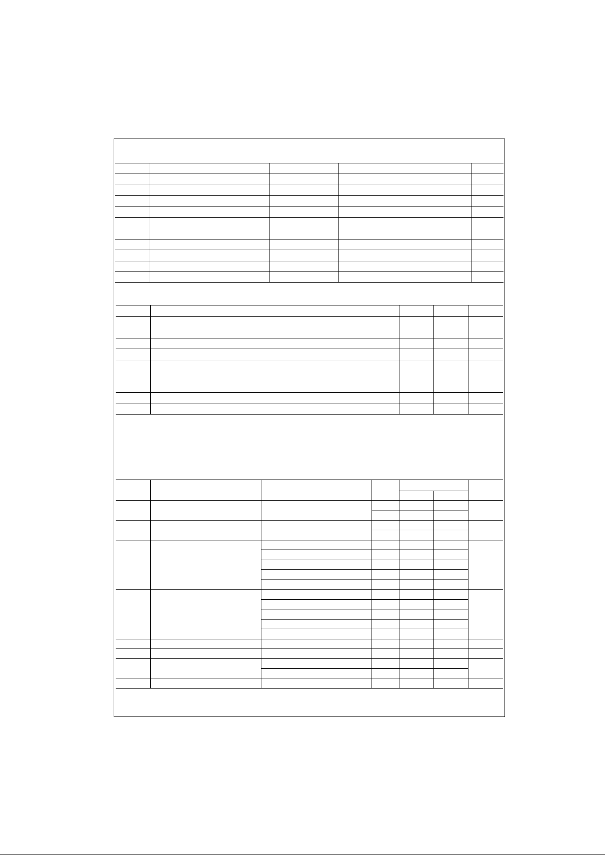
Absolute Maximum Ratings(Note 1)
Recommended Operating Conditions (Note 3)
Note 1: The Absolute Maximum Ratings are those values beyond which the safety of the device cannot be guaranteed. The device should not be operated
at these limits. Th e parametric values def ined in the Electrical Cha racteristic s tables are not guaran teed at the A bsolute Ma ximum Rating s. The “Rec ommended Operat ing Conditions” table will define the conditions fo r ac t ual device operation.
Note 2: I
O
Absolute Maximum Rating must be observed.
Note 3: Unused inputs must be held HIGH or LOW. They may not float.
DC Electrical Characteristics
Symbol Parameter Value Conditions Units
V
CC
Supply Voltage −0.5 to +7.0 V
V
I
DC Input Voltage −0.5 to +7.0 V
V
O
DC Output Voltage −0.5 to VCC + 0.5 Output in HIGH or LOW State (Note 2) V
I
IK
DC Input Diode Current −50 VI < GND mA
I
OK
DC Output Diode Current −50 VO < GND
mA
+50 V
O
> V
CC
I
O
DC Output Source/Sink Current ±50 mA
I
CC
DC Supply Current per Supply Pin ±100 mA
I
GND
DC Ground Cu rrent per Ground Pin ±100 mA
T
STG
Storage Temperature −65 to +150 °C
Symbol Parameter Min Max Units
V
CC
Supply Voltage Operating 2 .0 3.6
V
Data Retention 1.5 3.6
V
I
Input Voltage 05.5V
V
O
Output Voltage HIGH or LOW State 0 V
CC
V
I
OH/IOL
Output Current VCC = 3.0V − 3.6V ±24
mA
V
CC
= 2.7V − 3.0V ±12
V
CC
= 2.3V − 2.7V ±8
T
A
Free-Air Operating Temperature −40 85 °C
∆t/∆V Input Edge Rate, V
IN
= 0.8V–2.0V, VCC = 3.0V 0 10 ns/V
Symbol Parameter Conditions
V
CCTA
= −40°C to +85°C
Units
(V) Min Max
V
IH
HIGH Level Input Voltage 2.3 − 2.7 1.7
V
2.7 − 3.6 2.0
V
IL
LOW Level Input Voltage 2.3 − 2.7 0.7
V
2.7 − 3.6 0.8
V
OH
HIGH Level Output Voltage IOH = −100 µA2.3 − 3.6 VCC − 0.2
IOH = −8 mA 2.3 1.8
IOH = −12 mA 2.7 2.2
V
IOH = −18 mA 3.0 2.4
IOH = 24 mA 3.0 2.2
V
OL
LOW Level Output Voltage IOL = −100 µA2.3 − 3.6 0.2
IOL = 8 mA 2.3 0.6
V
IOL = 12 mA 2.7 0.4
IOL = 16 mA 3.0 0.4
IOL = 24 mA 3.0 0.55
I
I
Input Leakage Current 0 ≤ VI ≤ 5.5V 2.3 − 3.6 ±5.0 µA
I
OFF
Power-Off Leakage Current VI or VO = 5.5V 0 10 µA
I
CC
Quiescent Supply Current VI = VCC or GND 2.3 − 3.6 10
µA
3.6V ≤ VI ≤ 5.5V 2.3 − 3.6 ±10
∆I
CC
Increase in ICC per Input VIH = VCC −0.6V 2.3 − 3.6 500 µA
3 www.fairchildsemi.com
74LCX04
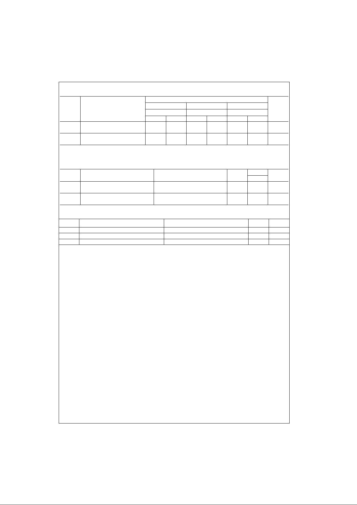
AC Electrical Characteristics
Note 4: Skew is def ined as the absolut e v alue of the difference between the actual propagation delay for any two separate outputs of the same device. The
specification applies t o any outputs switching in th e s am e direction, either HIG H -t o-LOW (t
OSHL
) or LOW-to-HIGH (T
OSLH
).
Dynamic Switching Characteristics
Capacitance
Symbol Parameter
TA = −40°C to +85°C, RL = 500Ω
Units
VCC = 3.3V ± 0.3V VCC = 2.7V VCC = 2.5V ± 0.2V
CL= 50 pF CL = 50 pF CL=30 pF
Min Max Min Max Min Max
t
PHL
Propagation Delay Time 1.5 5.2 1.5 6.0 1.5 6.2
ns
t
PLH
1.5 5.2 1.5 6.0 1.5 6 .2
t
OSHL
Output to Output Skew 1.0
ns
t
OSLH
(Note 4) 1.0
Symbol Parameter Conditions
V
CC
(V)
TA = 25°C
Units
Typical
V
OLP
Quiet Output Dynamic Peak V
OL
CL = 50 pF, VIH = 3.3V, VIL = 0V 3.3 0.8
V
CL = 30 pF, VIH = 2.5V, VIL = 0V 2.5 0.6
V
OLV
Quiet Output Dynamic Valley V
OL
CL = 50 pF, VIH = 3.3V, VIL = 0V 3.3 −0.8
V
CL = 30 pF, VIH = 2.5V, VIL = 0V 2.5 −0.6
Symbol Parameter Conditions Typical Units
C
IN
Input Capacitance VCC = Open, VI = 0V or V
CC
7pF
C
OUT
Output Capacitance VCC = 3.3V, VI = 0V or V
CC
8pF
C
PD
Power Dissipation Capacitance VCC = 3.3V, VI = 0V or VCC, f = 10 MHz 25 pF
 Loading...