Fairchild Semiconductor 74FR74SCX, 74FR74SC Datasheet

© 1999 Fairchild Semiconductor Corporation DS010977 www.fairchildsemi.com
March 1992
Revised August 1999
74FR74 • 74FR1074 Dual D-Type Flip-Flop
74FR74 • 74FR1074
Dual D-Type Flip-Flop
General Description
The 74FR74 and 74 FR107 4 are dua l D-ty pe flip-f lops with
true and complement (Q/Q
) outputs. On the 74F R74, data
at the D inputs is transferred t o the outputs on the rising
edge of the clock inpu t (CP
n
). The 74FR1074 is the neg a-
tive edge triggered version of this device. Both parts feature asynchronous clear (C
Dn
) and set (SDn) inputs which
are low level enabled.
Features
■ 74FR74 is pin-for-pin compatible with the 74F74
■ True 150 MHz f
MAX
capability on 74FR74
■ Outputs sink 24 mA and source 24 mA
■ Guarante ed pin-to-pin skew specifications
Ordering Code:
Devices also availab le in Tape and Reel. Specify by appending th e s uffix let t er “X” to the ordering code.
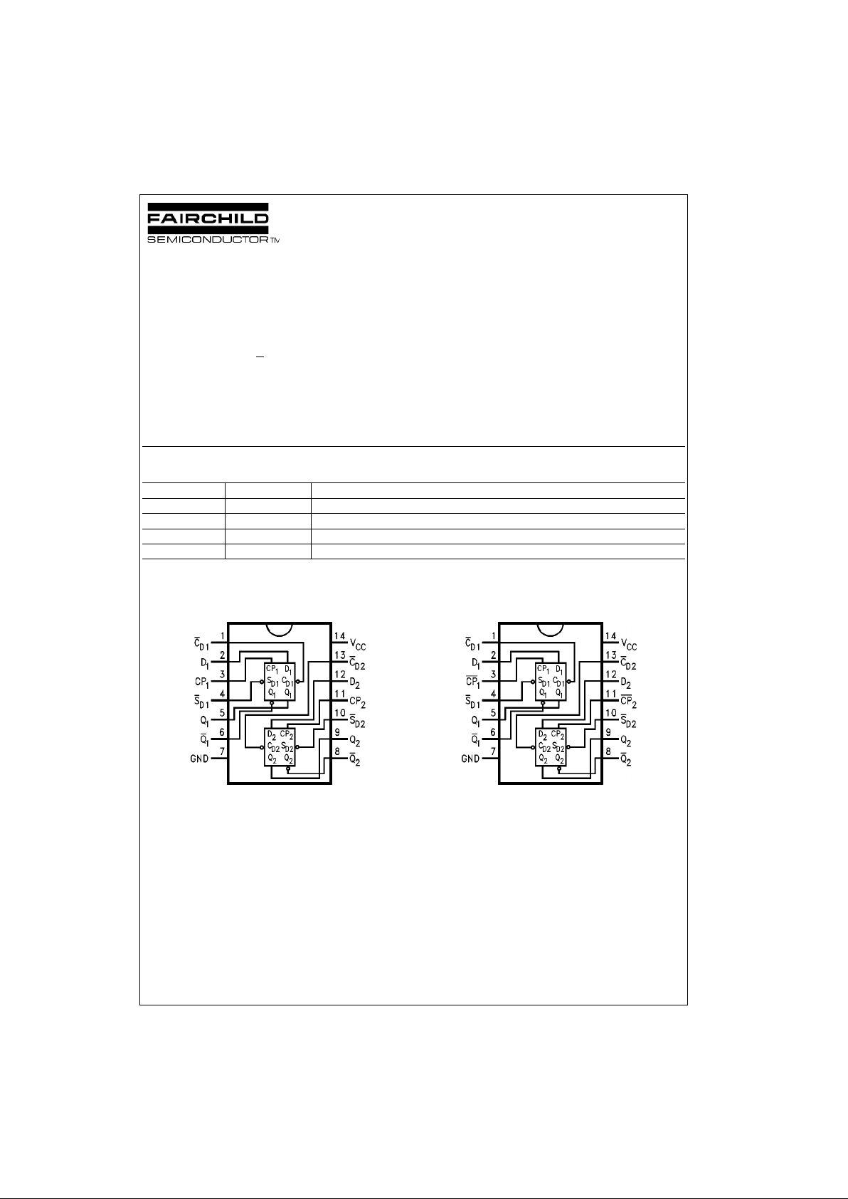
Connection Diagrams
74FR74 74FR1074
Order Number Package Number Package Description
74FR74SC M14A 14-Lead Small Outline Integrated Circuit (SOIC), JEDEC MS-120, 0.150 Narrow
74FR74PC N14A 14-Lead Plastic Dual-In-Line Package (PDIP), JEDEC MS-001, 0.300 Wide
74FR1074SC M14A 14-Lead Small Outline Integrated Circuit (SOIC), JEDEC MS-120, 0.150 Narrow
74FR1074PC N14A 14-Lead Plastic Dual-In-Line Package (PDIP), JEDEC MS-001, 0.300 Wide

www.fairchildsemi.com 2
74FR74 • 74FR1074
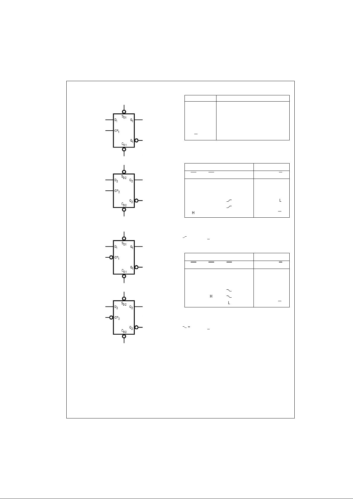
Logic Symbols
74FR74
74FR1074
Pin Descriptions
Tr uth Tables
74FR74
H = HIGH Voltage Level
L = LOW Voltage Level
Z = High Impedance
X = Immaterial
= Rising Edge
Q
0
= Previous Q(Q) before LOW-to-HIGH Clock Transition
74FR1074
H = HIGH Voltage Level
L = LOW Voltage Level
Z = High Impedance
X = Immaterial
= Falling Edge
Q
0
= Previous Q(Q) before HIGH-to-LOW Clock Transition
Pin Names Description
D
n
Data Inputs
CP
n
Clock Inputs
S
Dn
Asynchronous Set Inputs
C
Dn
Asynchronous Clear Inputs
Q
n
True Output
Q
n
Complementary Output
Inputs Outputs
SD
CD CP D Q Q
LHXXHL
HLXXLH
LLXXHH
HH
HH L
HH
LLH
HHLXQ
0
Q
0
Inputs Outputs
SD
CD CP DQ Q
LHXXHL
HLXXLH
LLXXHH
HH
HH L
HH
LLH
HHLXQ
0
Q
0

3 www.fairchildsemi.com
74FR74 • 74FR1074
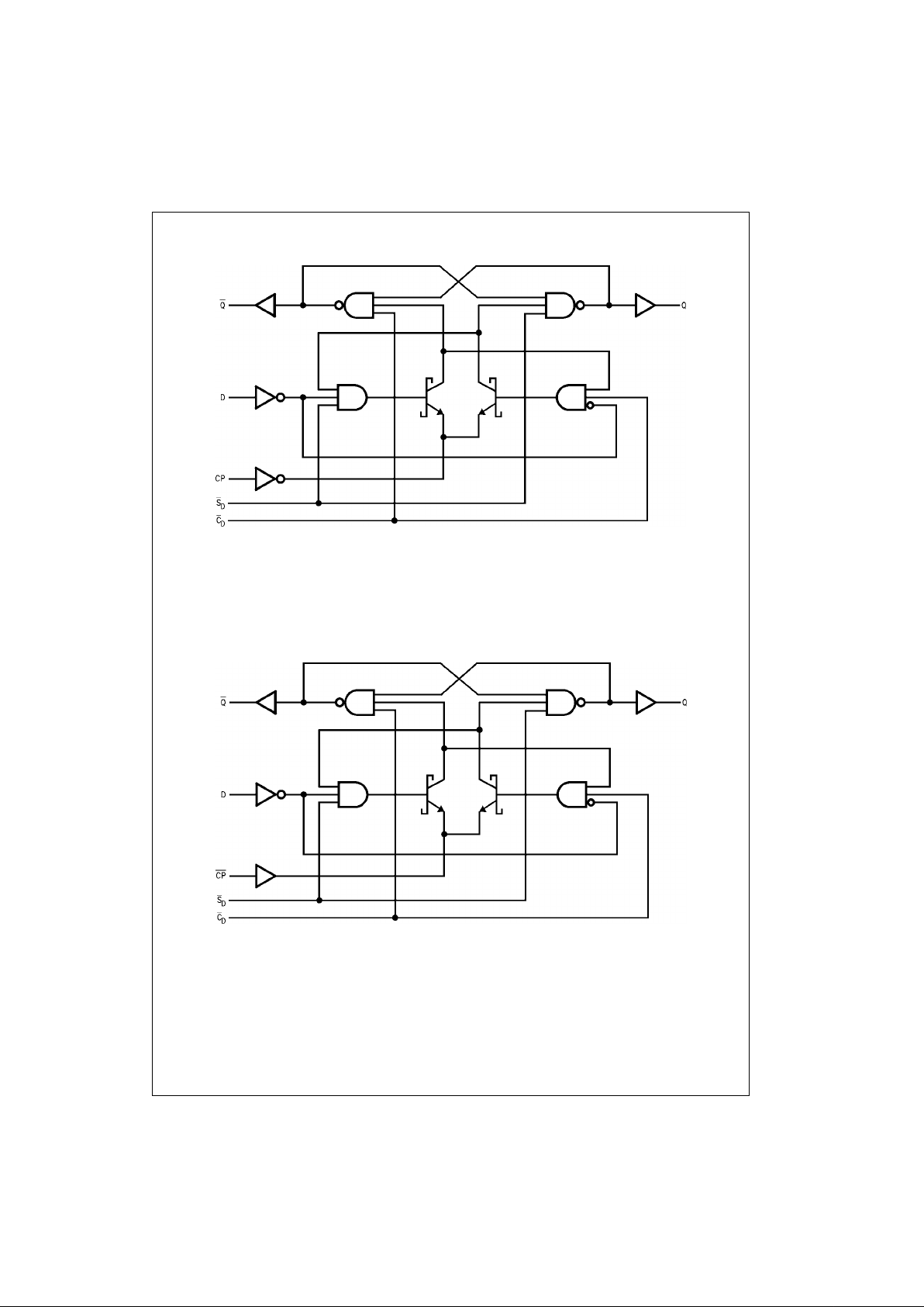
Logic Diagrams
74FR74
74FR1074
Please note that thes e diagrams are provide d only for the understan ding of logic operations a nd should not be used to es t im ate propagation delays.
 Loading...