

Fairchild Semiconductor 74FR543SPC, 74FR543SCX, 74FR543SC Datasheet
© 1999 Fairchild Semiconductor Corporation DS010902 www.fairchildsemi.com
January 1991
Revised August 1999
74FR543 Octal Latched Transceiver with 3-STATE Outputs
74FR543
Octal Latched Transceiver with 3-STATE Outputs
General Description
The 74FR543 octal tr ansc eiv er cont ains two sets of D-type
latches for temporary storage of data flowing in either
direction. Separate Latch Enable and Output Enable inputs
are provided for each reg ister to permit indep endent control of inputting and outputt ing in either direction of data
flow. Both the A and B outputs will source 15 mA and sink
64 mA.
Features
■ Functionally equivalent to 74F543
■ Back-to-back registers for storage
■ Bidirectional data path
■ A and B outputs have current sourcing capability of
15 mA and current sinking capability of 64 mA
■ Separate controls for data flow in each direction
■ Guarante ed pin-to-pin skew
■ Guarante ed 4000V minimum ESD protection
Ordering Code:
Devices also availab le in Tape and Reel. Specify by appending th e s uffix let t er “X” to the ordering code.
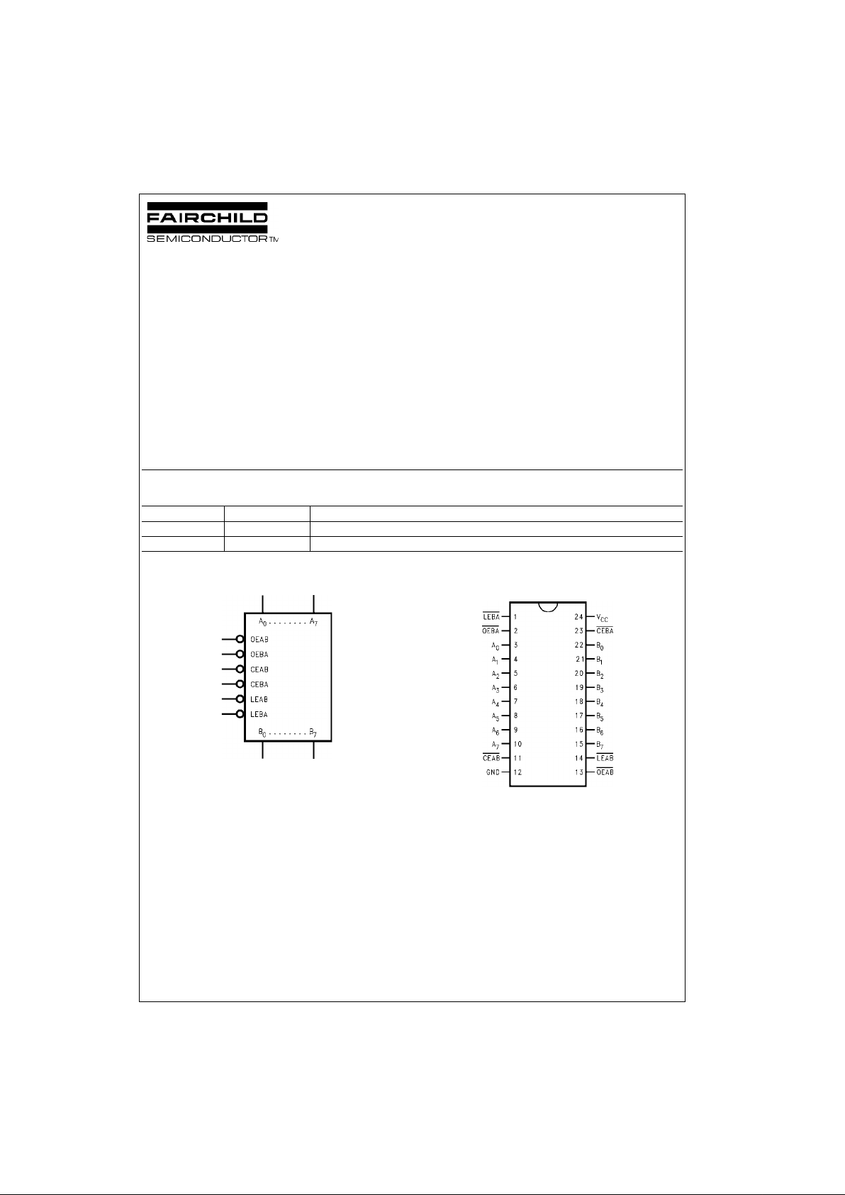
Logic Symbol Connection Diagram
Order Number Package Number Package Description
74FR543SC M24B 24-Lead Small Outline Integrated Circuit (SOIC), JEDEC MS-013, 0.300 Wide
74FR543SPC N24C 24-Lead Plastic Dual-In-Line Package (PDIP), JEDEC MS-100, 0.300 Wide
www.fairchildsemi.com 2
74FR543
Pin Descriptions
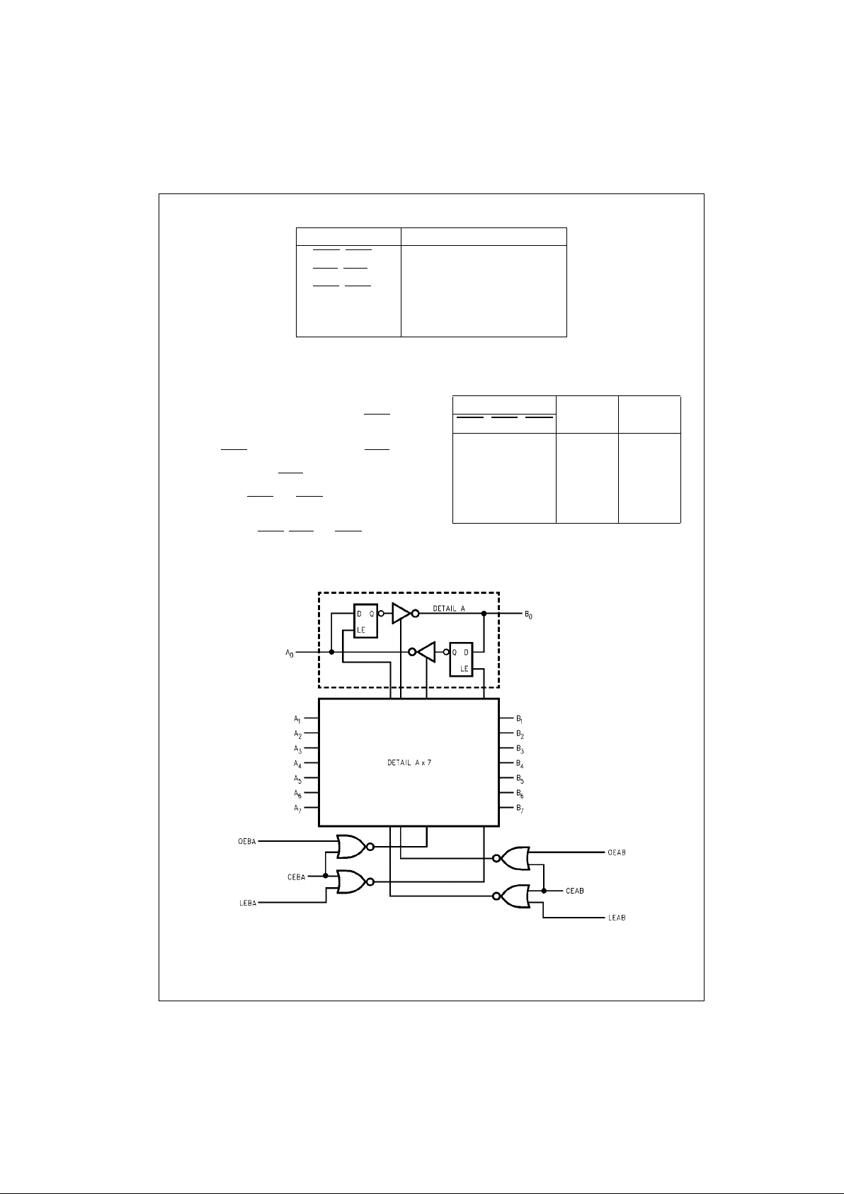
Functional Description
The 74FR543 contains two sets of D-type latches, with
separate input and outp ut controls for each. For data flow
from A-to-B, fo r example, t he A-to-B E nable (CEA B
) input
must be LOW in order to enter data from the A Port or take
data from the B Port as indi cated in the Data I/O Control
Table. With CEAB
LOW, a LOW signal on (LEAB) input
makes the A-to-B latc he s tra nsp are nt; a sub seq ue nt L OWto-HIGH transition of the LEAB
line puts the A latches in
the storage mode an d their outputs n o longer ch ange with
the A inputs. With CEAB
and OEAB both LOW, the B ou tput buffers are active and reflect the data pres ent on the
output of the A latches. Control of data flow from B-to-A is
similar, but using the CEBA
, LEBA and OEBA.
Data I/O Control Table
H = HIGH Voltage Level
L = LOW Voltage Level
X = Immaterial
Logic Diagram
Pin Names Description
OEAB
, OEBA Output Enable Inputs
LEAB
, LEBA Latch Enable Inputs
CEAB
, CEBA Chip Enable Inputs
A
0–A7
Side A Inputs or 3-STATE Outputs
B
0–B7
Side B Inputs or 3-STATE Outputs
Inputs Latch Output
CEAB
LEAB OEAB Status Buffers
H X X Latched High Z
X H X Latched —
L L X Transparent —
XXH — High Z
L X L — Driving
 Loading...