

Fairchild Semiconductor 74FR25900SSCX, 74FR25900SSC Datasheet
© 1999 Fairchild Semiconductor Corporation DS011500 www.fairchildsemi.com
July 1992
Revised August 1999
74FR25900 9-Bit, 3-Port Latchable Datapath Multiplexer
74FR25900
9-Bit, 3-Port Latchable Datapath Multiplexer
with 25Ω Output Series Resistors
General Description
The 74FR25900 is a data bus multiplexer routing a ny of
three 9-bit ports to any other one o f the three ports. Readback of data latched from an y port on to itself is also possi ble. The 74FR25900 maintains separate control of all latchenable, output enable and se lect inputs for maximum flexibility. PINV allows inversion of the data from the C
8
to A8 or
B
8
path. This is useful for control of the parity bit in systems
diagnostics.
This device includes 25Ω resist ors in series with A and B
Port outputs. Resistors minimize undershoot and ringing
which may damage or corrupt sensitive device inputs
driven by these ports.
Features
■ 25Ω series resistors in th e port A and B outputs elimi-
nate the need for external resistors when driving MOS
inputs such as DRAM arrays
■ 9-bit data ports for systems carrying parity bits
■ Readback capability for system self checks.
■ Independent control lines for maximum flexibility
■ Guaranteed multiple ou tput switching and 250 pF load
delays
■ Outputs optimized for dynamic bus drive capability
■ PINV parity control facilitates system diagnostics
■ 74FR900 op tion available without output series resistors
Ordering Code:
Devices also availab le in Tape and Reel. Specify by appending th e s uffix let t er “X” to the ordering cod e.
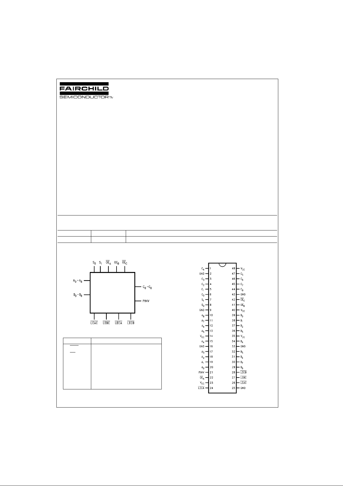
Logic Symbol
Pin Description
Connection Diagram
Order Number Package Number Package Description
74FR25900SSC MS48A 48-Lead Small Shrink Outline Package (SSOP), JEDEC MO-118, 0.300 Wide
Pin Names Description
LExx
Latch Enable Inputs
OE
x
Output Enable Inputs
PINV Parity Invert Input
S
0
, S
1
Select Inputs
A
0–A8
Port A Inputs or 3-STATE Outputs
B
0–B8
Port B Inputs or 3-STATE Outputs
C
0–C8
Port C Inputs or 3-STATE Outputs
www.fairchildsemi.com 2
74FR25900
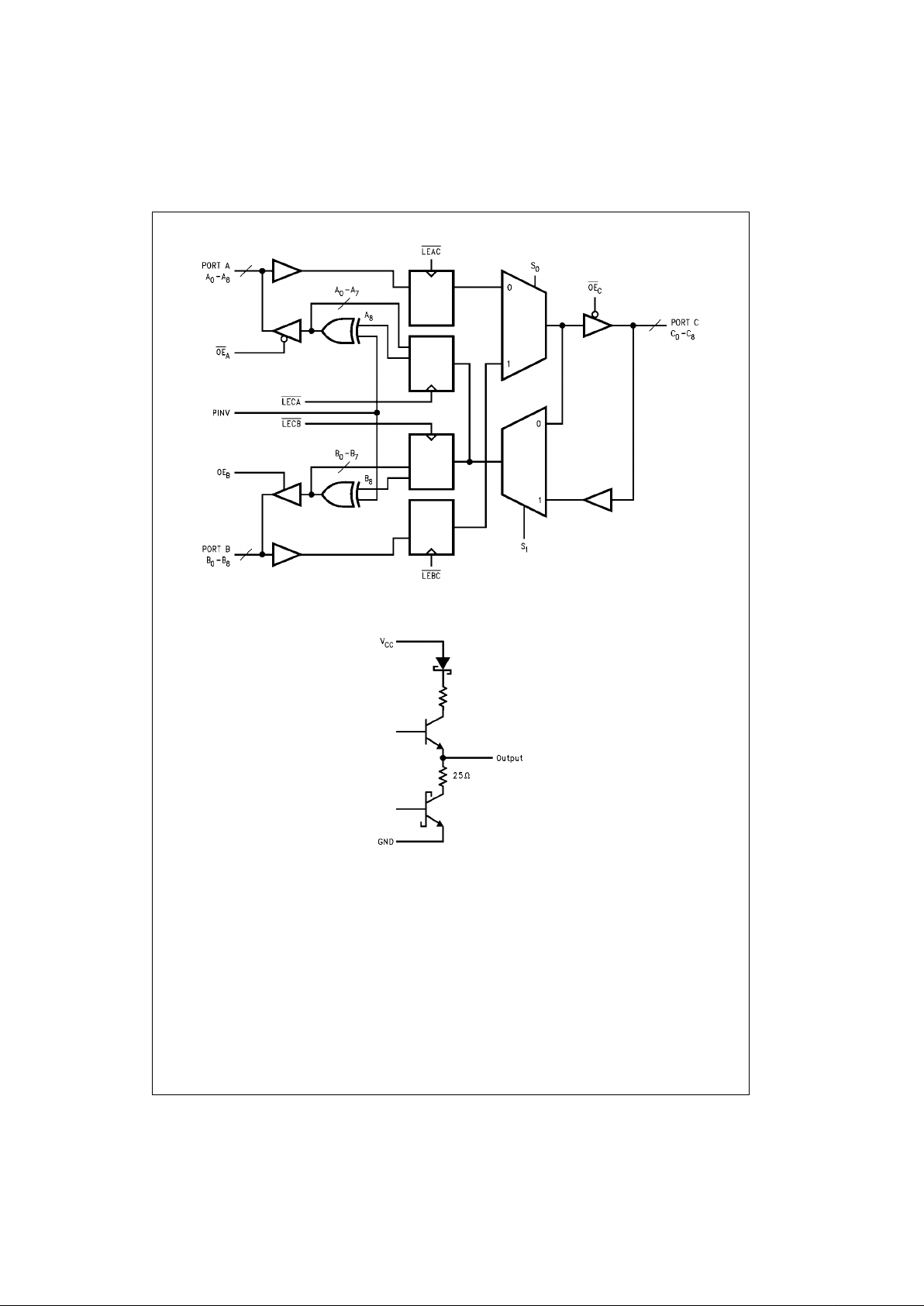
Functional Description
The 74FR25900 allows 9-bit data to be transferred from
any of three 9-bit I/O ports to either of the two remaining
I/O ports. The device employs latches in all paths for either
transparent or synchronous operation. Readback capability
from any port to itself is also possible.
Data transfer within the 74FR 25900 is controlled through
use of the select (S
0
and S1) and output-enable (OEA, OE
B
and OEC) inputs as described in Table 1. Additional control
is available by use of the latch-enable inputs (LEAC
, LECA,
LEBC
, LECB) allowing either synchronous or transparent
transfers (see Table 2). Table 1 indicates several readback
conditions. By latchi ng data on a given por t and initiating
the readback control configu ration, previous data may be
read for system verificatio n or diag nostics. T his mode m ay
be useful in implementing system diagnostics.
Data at the port t o be readback must be latched prior to
enabling the outputs on that port. If this is not done, a
closed data loop will result causing possible data integ rity
problems. Note that the A and B Ports allow readback without affecting any other port. C Port, however, requires interruption of either A or B Ports to complete its readback path.
PINV controls inversion of the C
8
bit. A LOW on PINV
allows C
8
data to pass unaltered. A HIGH causes inversion
of the data. See Table 3. This feature allows forcing of parity errors for use in s ystem diagnostics. This is particula rly
helpful in 486 processor desi gns as the 486 does not pro vide odd/e ven parity s election internally.
TABLE 1. Datapath Control
Note 1: Readback operation in latc hed mode only. Transparent opera tion
could result in unpredictable results.
TABLE 2. Latch-Enable Control
TABLE 3. PINV Control
Key:
L = LOW Voltage
H = HIGH Voltage Level
Q
0
= Output state prior t o LExx LOW-to-HIGH transition
Inputs
Function
S
0S1
OEAOEBOE
C
L X H L L Port A to Port C
L L H H H Port A to Port B
L O H H L Port A to B+C
H L L L H Port B to Port A
H X H L L Port B to Port C
H O L L L Port B to A+C
X H L L H Port C to Port A
X H H H H Port C to Port B
X H L H H Port C to A+B
X X H L H Outputs Disabled
L L L X X (Readback to A)
(Note 1)
L H L X L (Readback to A or C)
(Note 1)
H L X H X (Readback to B)
(Note 1)
H H X H L (Readback to B or C)
(Note 1)
LExx
Input Out put
LLL
LHH
HXQ
0
PINV C
8
A8 or B
8
LLL
LHH
HLH
HHL
3 www.fairchildsemi.com
74FR25900
Logic Diagram
Schematic of A and B Port Outputs
 Loading...