


Fairchild Semiconductor 74FR2244SJ, 74FR2244SCX, 74FR2244SC, 74FR2244PC Datasheet
© 1999 Fairchild Semiconductor Corporation DS010931 www.fairchildsemi.com
June 1991
Revised August 1999
74FR2244 Octal Buffer/Line Driver
74FR2244
Octal Buffer/Line Driver
with 25Ω Series Resistors in the Outputs
General Description
The 74FR2244 is a non-inverting octal buffer and line driver
designed to drive capacitive inputs of MOS memory
devices, address and clock line s or act as a low undershoot general purpose bus driver.
Features
■ 3-STATE outputs drive bus lines or buffer memory
address registers
■ Outputs sink 12 mA and source 15 mA
■ 25Ω series resistors in outputs eliminate the need for
external resistors
■ Designed to drive the capacitive inputs of MOS devices
Ordering Code:
Devices also availab le in Tape and Reel. Specify by appending th e s uffix let t er “X” to the ordering code.
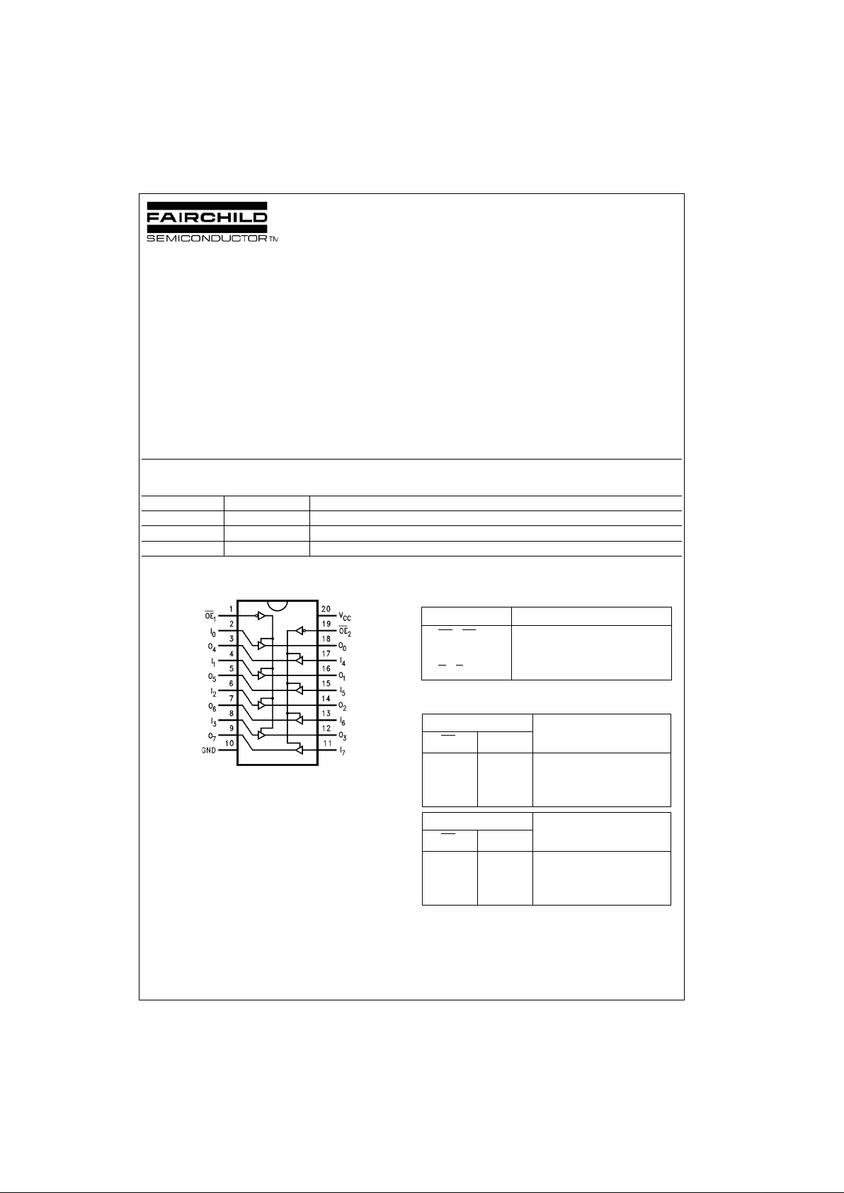
Connection Diagram Pin Descriptions
Truth Tables
H = HIGH Voltage Level
L = LOW Voltage Level
X = Immaterial
Z = High Impedance
Order Number Package Number Package Description
74FR2244SC M20B 20-Lead Small Outline Integrated Circuit (SOIC), JEDEC MS-013, 0.300 Wide
74FR2244SJ M20D 20-Lead Small Outline Package (SOP), EIAJ TYPE II, 5.3mm Wide
74FR2244PC N20A 20-Lead Plastic Dual-In-Line Package (PDIP), JEDEC MS-001, 0.300 Wide
Pin Names Description
OE
1
, OE
2
Output Enable Input (Active-LOW)
I
0–I7
Inputs
O
0–O7
Outputs
Inputs Outputs
OE
1
I
n
(Pins 12, 14, 16, 18)
LL L
LH H
HX Z
Inputs Outputs
OE
2
I
n
(Pins 3, 5, 7, 9)
LL L
LH H
HX Z
www.fairchildsemi.com 2
74FR2244
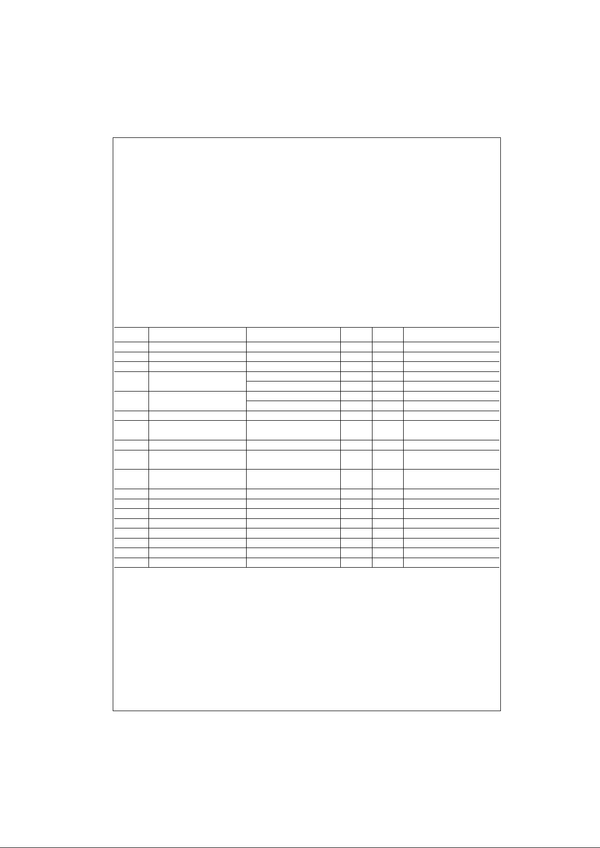
Absolute Maximum Ratings(Note 1) Recommended Operating
Conditions
Note 1: Absolute maximum ratings are values beyond which the device
may be damaged or have its useful life impai red.
Note 2: Either voltage limit or curren t limit is sufficient to protect in put s .
DC Electrical Characteristics
Storage Temperature −65°C to +150°C
Ambient Temperature under Bias −55°C to +125°C
Junction Temperature under Bias −55°C to +150°C
V
CC
Pin Potential to Ground Pin −0.5V to +7.0V
Input Voltage (Note 2) −0.5V to +7.0V
Input Current (Note 2) −30 mA to +5.0 mA
Voltage Applied to Output
in HIGH State (with V
CC
= 0V)
Standard Output −0.5V to V
CC
3-STATE Output −0.5V to +5.5V
Current Applied to Output
in LOW State (Max) Twice the Rated I
OL
(mA)
ESD Last Passing Voltage (Min) 4000V
Free Air Ambient Temperature 0°C to +70°C
Supply Voltage +4.5V to +5.5V
Symbol Parameter Min Typ Max Units
V
CC
Conditions
V
IH
Input HIGH Voltage 2.0 V Recognized HIGH Signal
V
IL
Input LOW Voltage 0.8 V Recognized LOW Signal
V
CD
Input Clamp Diode Voltage −1.2 V Min IIN = −18 mA
V
OH
Output HIGH Voltage 2.4 V Min IOH = −3 mA
2.0 V Min IOH = −15 mA
V
OL
Output LOW Voltage 0.5 V Min IOL = 1 mA
0.75 V Min IOL = 12 mA
I
IH
Input HIGH Current 5 µAMaxVIN = 2.7V
I
BVI
Input HIGH Current 7 µAMaxVIN = 7.0V
Breakdown Test
I
IL
Input LOW Current −150 µAMaxVIN = 0.5V
V
ID
Input Leakage Test 4.75 V 0.0 IID = 1.9 µA
All Other Pins Grounded
I
OD
Output Circuit Leakage Current 3.75 µA0.0V
IOD
= 150 mV
All Other Pins Grounded
I
OZH
Output Leakage Current 20 µAMaxV
OUT
= 2.7V
I
OZL
Output Leakage Current −20 µAMaxV
OUT
= 0.5V
I
OS
Output Short-Circuit Current −100 −225 mA Max V
OUT
= 0.0V
I
CEX
Output HIGH Leakage Current 50 µAMaxV
OUT
= V
CC
I
ZZ
Bus Drainage Test 100 µA0.0V
OUT
= 5.25V
I
CCH
Power Supply Current 40 mA Max All Outputs HIGH
I
CCL
Power Supply Current 70 mA Max All Outputs LOW
I
CCZ
Power Supply Current 46 mA Max Outputs 3-STATE