

Fairchild Semiconductor 74FR2240SCX, 74FR2240SC, 74FR2240PC Datasheet
© 1999 Fairchild Semiconductor Corporation DS010904 www.fairchildsemi.com
January 1991
Revised August 1999
74FR2240 Octal Buffer/Line Driver
74FR2240
Octal Buffer/Line Driver
with 25Ω Series Resistors in the Outputs
General Description
The 74FR2 240 is an inverting octal buffer and line driver
designed to drive capacitive inputs of MOS memory
devices, address and clock line s or act as a low undershoot general purpose bus driver.
Features
■ 3-STATE outputs drive bus lines or buffer memory
address registers
■ Outputs sink 12 mA and source 15 mA
■ 25Ω series resistors in outputs eliminate the need for
external resistors
■ Designed to drive the capacitive inputs of MOS devices
Ordering Code:
Devices also availab le in Tape and Reel. Specify by appending th e s uffix let t er “X” to the ordering code.
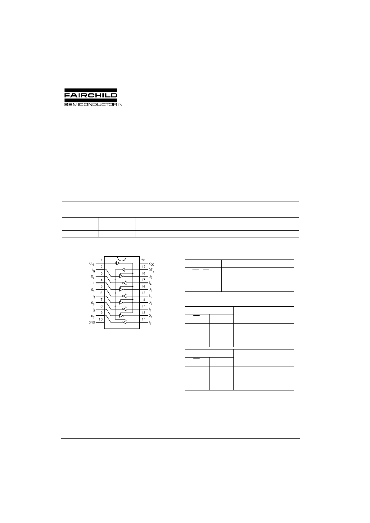
Connection Diagram Pin Descriptions
Truth Tables
H = HIGH Voltage Level
L = LOW Voltage Level
X = Immaterial
Z = High Impedance
Order Number Package Number Package Description
74FR2240SC M20B 20-Lead Small Outline Integrated Circuit (SOIC), JEDEC MS-013, 0.300 Wide
74FR2240PC N20A 20-Lead Plastic Dual-In-Line Package (PDIP), JEDEC MS-001, 0.300 Wide
Pin Names Description
OE
1
, OE
2
Output Enable Input (Active-LOW)
I
0–I7
Inputs
O
0–O7
Outputs
Inputs Outputs
OE
1
I
n
(Pins 12, 14, 16, 18)
LL H
LH L
HX Z
Inputs Outputs
OE
2
I
n
(Pins 3, 5, 7, 9)
LL H
LH L
HX Z

www.fairchildsemi.com 2
74FR2240
Absolute Maximum Ratings(Note 1) Recommended Operating
Conditions
Note 1: Absolute maximum ratings are values beyond which the device
may be damaged or have its useful life impaired. Functional operation
under these conditi ons is not implied.
Note 2: Either voltage limit or curren t limit is sufficient to protect in put s .
DC Electrical Characteristics
Storage Temperature −65°C to +150°C
Ambient Temperature under Bias −55°C to +125°C
Junction Temperature under Bias −55°C to +150°C
V
CC
Pin Potential to Ground Pin −0.5V to +7.0V
Input Voltage (Note 2) −0.5V to +7.0V
Input Current (Note 2) −30 mA to +5.0 mA
Voltage Applied to Output
in HIGH State (with V
CC
= 0V)
Standard Output −0.5V to V
CC
3-STATE Output −0.5V to +5.5V
Current Applied to Output
in LOW State (Max) Twice the Rated I
OL
(mA)
ESD Last Passing Voltage (Min) 4000V
Free Air Ambient Temperature 0°C to +70°C
Supply Voltage +4.5V to +5.5V
Symbol Parameter Min Typ Max Units
V
CC
Conditions
V
IH
Input HIGH Voltage 2.0 V Recognized HIGH Signal
V
IL
Input LOW Voltage 0.8 V Recognized LOW Signal
V
CD
Input Clamp Diode Voltage −1.2 V Min IIN = −18 mA
V
OH
Output HIGH Voltage 2.4 V Min IOH = −3 mA
2.0 V Min IOH = −15 mA
V
OL
Output LOW Voltage 0.5 V Min IOL = 1 mA
0.75 V Min IOL = 12 mA
I
IH
Input HIGH Current 5 µAMaxVIN = 2.7V
I
BVI
Input HIGH Current
7 µAMaxVIN = 7.0V
Breakdown Test
I
IL
Input LOW Current −150 µAMaxVIN = 0.5V
V
ID
Input Leakage Test 4.75 V 0.0 IID = 1.9 µA
All Other Pins Grounded
I
OD
Output Circuit Leakage Current 3.75 µA0.0V
IOD
= 150 mV
All Other Pins Grounded
I
OZH
Output Leakage Current 20 µAMaxV
OUT
= 2.7V
I
OZL
Output Leakage Current −20 µAMaxV
OUT
= 0.5V
I
OS
Output Short-Circuit Current −100 −225 mA Max V
OUT
= 0.0V
I
CEX
Output HIGH Leakage Current 50 µAMaxV
OUT
= V
CC
I
ZZ
Bus Drainage Test 100 µA0.0V
OUT
= 5.25V
I
CCH
Power Supply Current 9 13 mA Max All Outputs HIGH
I
CCL
Power Supply Current 37 45 mA Max All Outputs LOW
I
CCZ
Power Supply Current 30 38 mA Max Outputs 3-STATE
 Loading...