

Fairchild Semiconductor 74FR16541SSCX, 74FR16541SSC, 74FR16541QC Datasheet
© 1999 Fairchild Semiconductor Corporation DS010616 www.fairchildsemi.com
October 1989
Revised August 1999
74FR16541 16-Bit Buffer/Line Driver with 3-STATE Outputs
74FR16541
16-Bit Buffer/Line Driver with 3-STATE Outputs
General Description
The 74FR16541 contains sixteen non-inverting buffers with
3-STATE outputs designed to be emplo yed as a memory
and address driver, clock driver, or bus-oriented tra nsmitter/receiver. The device is byte co ntrolled. Each byte has
separate 3-STATE control inputs which can be shorted
together for full 16-bit operation.
Features
■ Non-inverting buffers
■ 3-STATE outputs drive bus lines
■ Output sink capability of 64 mA, source capability of
15 mA
■ Separate 3-STATE control pins for each byte
■ Guaranteed multiple output switching, 250 pF delays
and pin-to-pin skew
■ 16-bit version of the 74F541, 74F244 or 74FR244
Ordering Code:
Devices also availab le in Tape and Reel. Specify by appending th e s uffix let t er “X” to the ordering code.
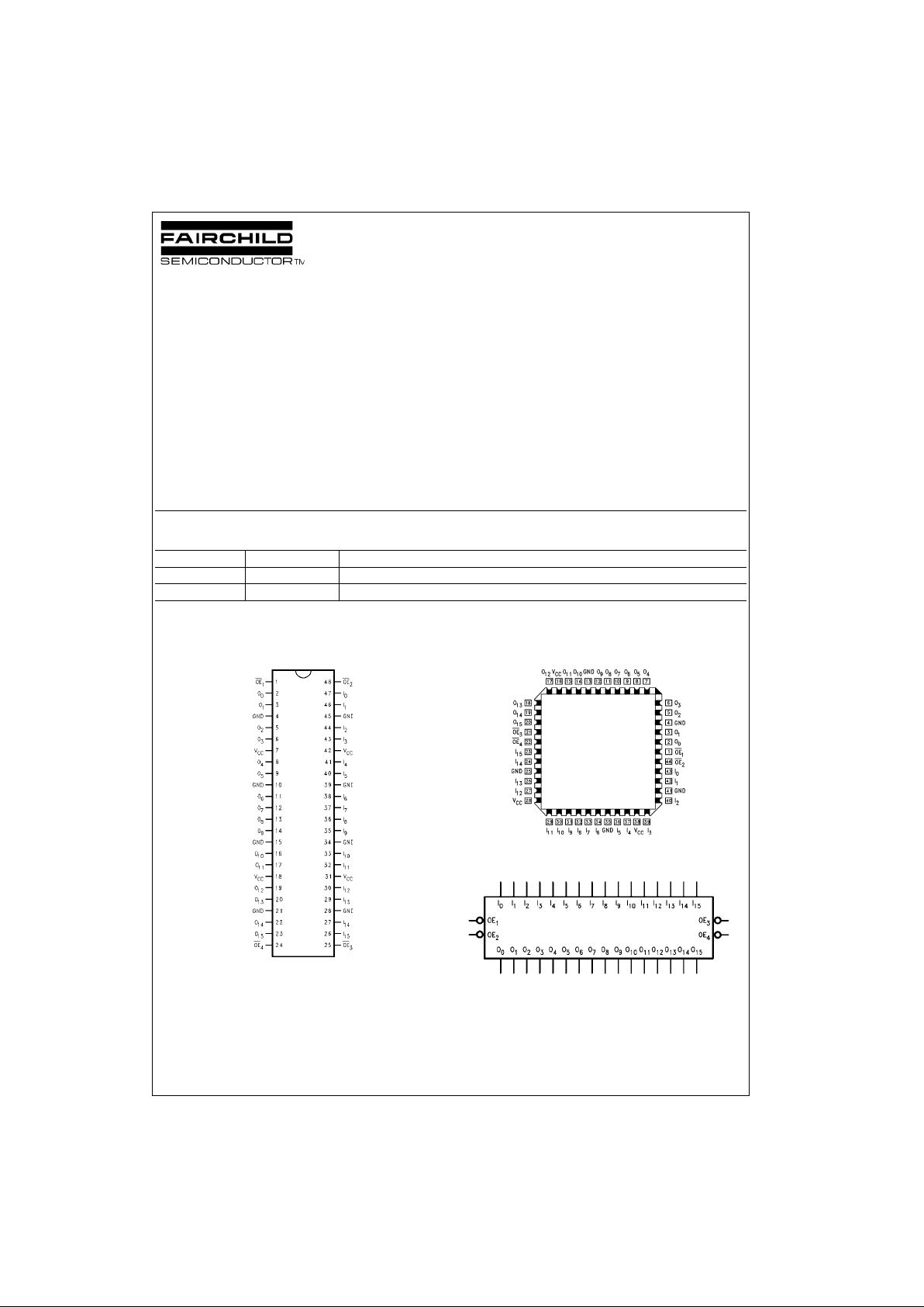
Connection Diagrams
Pin Assignment for SSOP Pin Assignment for PLCC
Logic Symbol
Order Number Package Number Package Description
74FR16541QC V44A 44-Lead Plastic Lead Chip Carrier (PLCC), JEDEC MO-047, 0.650 Square
74FR16541SSC MS48A 48-Lead Small Shrink Outline Package (SSOP), JEDEC MO-118, 0.300 Wide
www.fairchildsemi.com 2
74FR16541
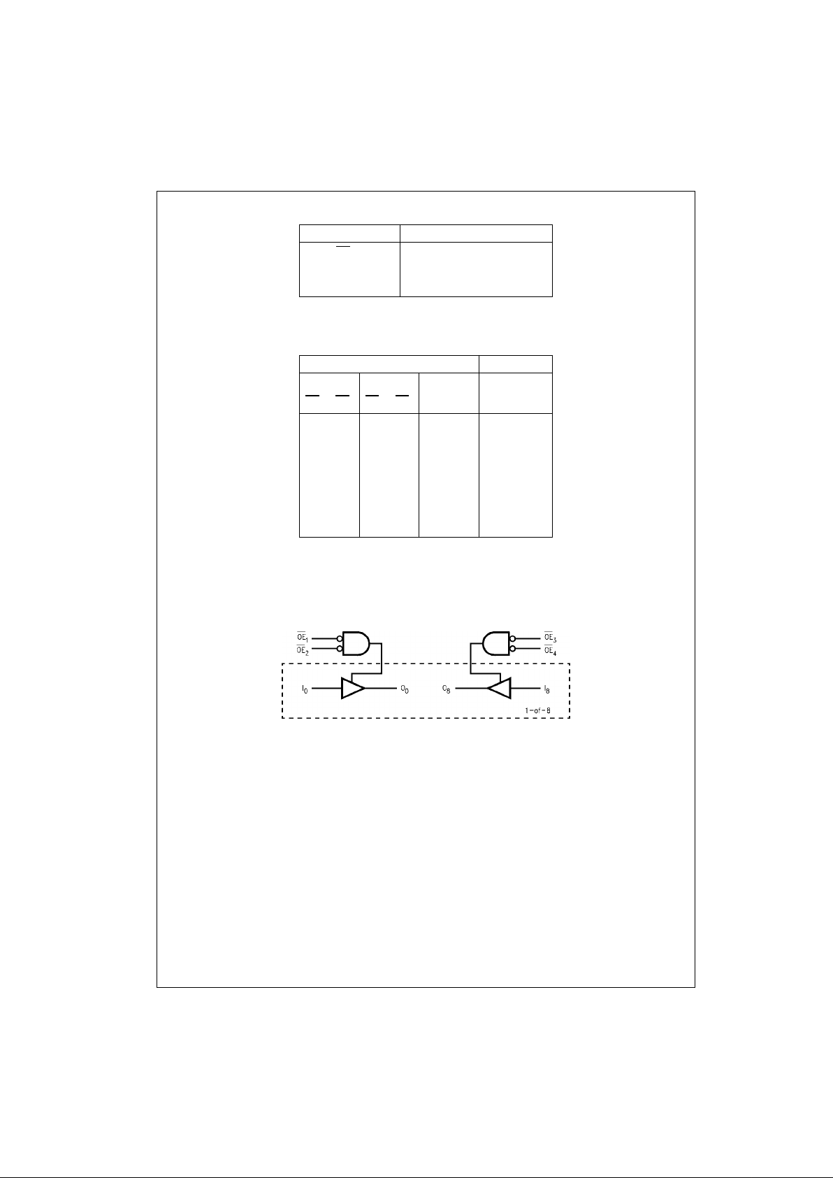
Pin Descriptions
Truth Table
H = HIGH Voltage Level
L = LOW Voltage Level
X = Immaterial
Z = High Impedance
Logic Diagram
Pin Names Description
OE
n
Output Enable Inputs
I
0–I15
Inputs
O
0–O15
3-STATE Outputs
Inputs Outputs
Byte1 [0:7] Byte2 [8:15] I
0–I7I8–I15O0–O7O8–O15
OE1OE2OE3OE
4
LLLLHHH H
HXL LXL Z L
XHL LXH Z H
LLHXLXL Z
LLXHHXH Z
HHHHXX Z Z
LLLLLL L L
 Loading...