

Fairchild Semiconductor 74FR16245SSCX, 74FR16245SSC, 74FR16245QC Datasheet
© 1999 Fairchild Semiconductor Corporation DS010614 www.fairchildsemi.com
October 1989
Revised August 1999
74FR16245 16-Bit Transceiver with 3-STATE Outputs
74FR16245
16-Bit Transceiver with 3-STATE Outputs
General Description
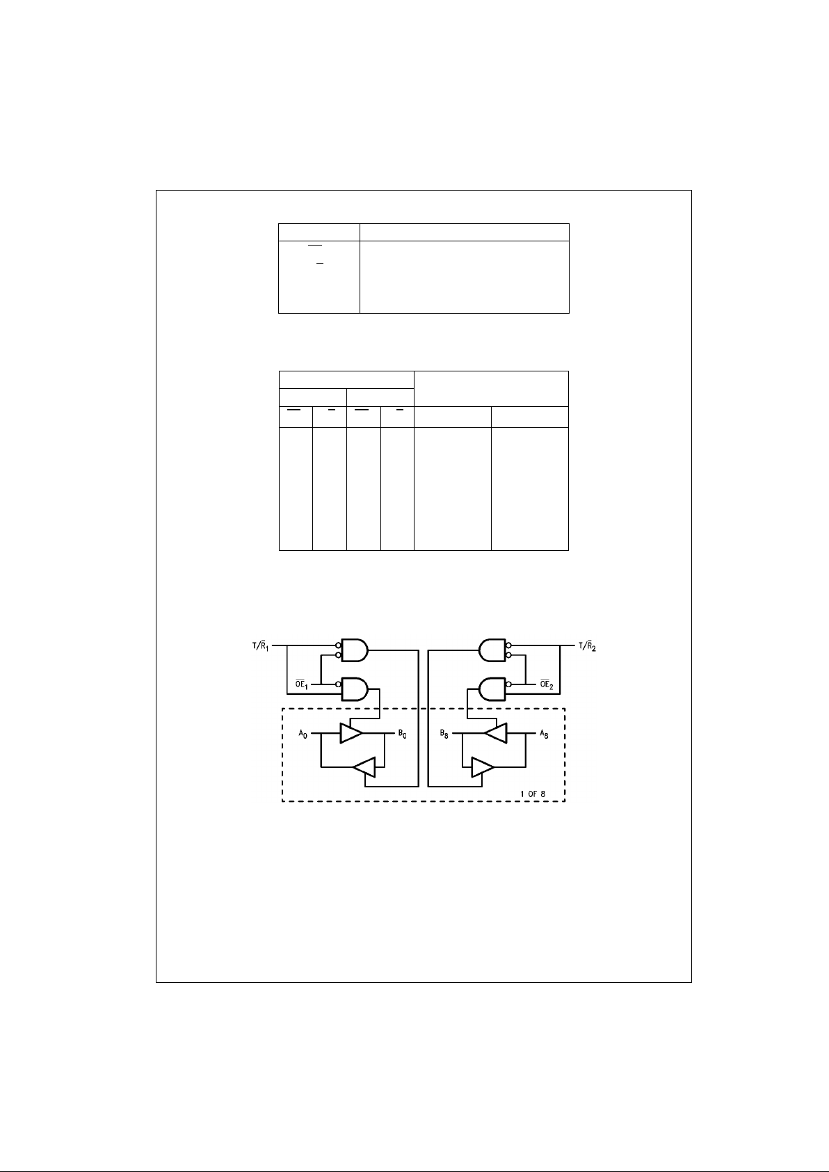
The 74FR16245 contains sixteen non-inverting bidirectional bu ffers with 3 -S TATE outpu t s an d is i nt e nd ed fo r b usoriented applications. Current sinking capability is 64 mA
on both the A and B Ports. The d evice is byte controlle d.
Each byte has separate control inputs which can be
shorted together for full 16-bit operation. The transmit/
receive (T/R
n
) inputs determine the dire ction of data flow
through the transceiver. The output enable (OE
n
) inputs
disable both A and B Ports by placing them in an high
impedance state.
Features
■ Non-inverting buffers
■ Bidirectional data paths
■ A and B output sink capability of 64 mA, source
capability of 15 mA
■ Separate control pins for each byte
■ Guarante ed pin-to-pin skew
■ Low 3-STATE I
IL
■ 16-Bit version of the 74F245 or 74F645
Ordering Code:
Devices also availab le in Tape and Reel. Specify by appending th e s uffix let t er “X” to the ordering code.
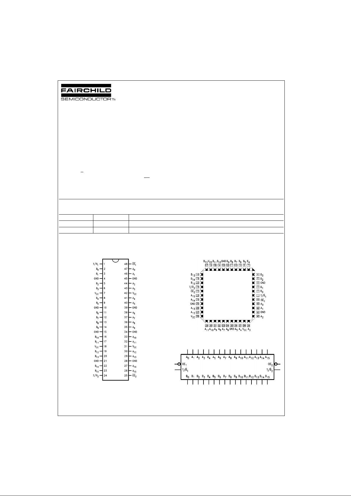
Connection Diagrams
Pin Assignment for SSOP Pin Assignment for PLCC
Logic Symbol
Order Number Package Number Package Description
74FR16245QC V44A 44-Lead Plastic Lead Chip Carrier (PLCC), JEDEC MO-047, 0.650 Square
74FR16245SSC MS48A 48-Lead Small Shrink Outline Package (SSOP), JEDEC MO-118, 0.300 Wide
www.fairchildsemi.com 2
74FR16245
Pin Descriptions
Truth Table
H = HIGH Voltage Level
L = LOW Voltage Level
X = Immaterial
Logic Diagram
Pin Names Description
OE
n
Output Enable Input
T/R
n
Transmit/Receive Input
A
0–A15
A Bus Inputs/3-STATE Outputs
B
0–B15
B Bus Inputs/3-STATE Outputs
Inputs Output Operating Mode
Byte1 (0:7) Byte2 (8:15)
OE
1
T/R1OE2T/R2Byte1 (0:7) Byte2 (8:15)
L L H X Bus B Data to A High Z State
L H H X Bus A Data to B High Z State
H X L L High Z State Bus B Data to A
H X L H High Z State Bus A Data to B
L L L L Bus B Data to A Bus B Data to A
L H L H Bus A Data to B Bus A Data to B
H X H X High Z State High Z State
 Loading...