Fairchild Semiconductor 74F899SCX, 74F899SC, 74F899QCX, 74F899QC, 74F899PC Datasheet

© 1999 Fairchild Semiconductor Corporation DS010195 www.fairchildsemi.com
February 1989
Revised August 1999
74F899 9-Bit Latchable Transceiver
74F899
9-Bit Latchable Transceiver
with Parity Generator/Checker
General Description
The 74F899 is a 9-bi t to 9-bit pa rity transcei ver with t ransparent latches. The device can operate as a feed-thr ough
transceiver or it can generat e/check parity from the 8-bit
data busses in either d i rect ion. It ha s a guaranteed curre nt
sinking capability of 24 mA at the A-bus and 64 mA a t the
B-bus.
The 74F899 features independent latch enables for the
A-to-B direction an d the B-to-A direction, a sel ect pin for
ODD/EVEN
parity, and separate error signal output pins for
checking parity.
Features
■ Latchable transceiver with output sink of 24 mA at the
A-bus and 64 mA at the B-bus
■ Option to select generate parity and check or
“feed-through” data/parity in directions A-to-B or B-to-A
■ Independent latch enables for A-to-B and B-to-A
directions
■ Select pin for ODD/EVEN
parity
■ ERRA
and ERRB output pins for parity checking
■ Ability to simultaneously generate and check parity
■ May be used in systems applications in place of the
74F543 and 74F280
■ May be used in system applications in place of the
74F657 and 74F3 73 (no need to chang e T/R
to check
parity)
Ordering Code:
Devices also availab le in Tape and Reel. Specify by appending th e s uffix let t er “X” to the ordering code.
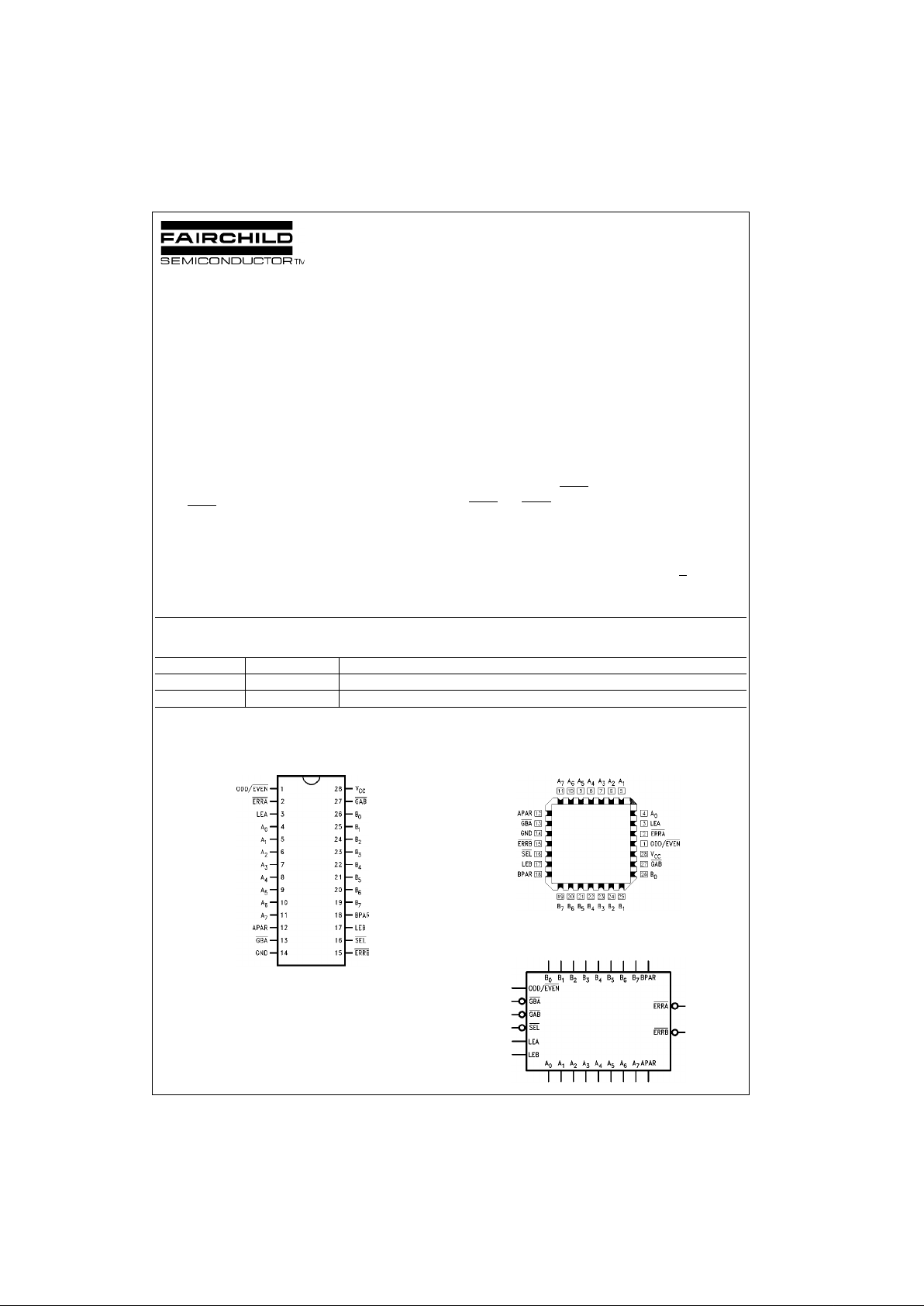
Connection Diagrams
Pin Assignment for SOIC Pin Assignment for PCC
Logic Symbol
Order Number Package Number Package Description
74F899SC M28B 28-Lead Small Outline Integrated Circuit (SOIC), JEDEC MS-013, 0.300 Wide
74F899QC V28A 28-Lead Plastic Lead Chip Carrier (PLCC), JEDEC MO-047, 0.450 Square

www.fairchildsemi.com 2
74F899
Input Loading/Fan-Out
Pin Descriptions
Functional Description
The 74F899 has t hree principal modes of ope ration which
are outlined below. These modes a pply to both the A -to-B
and B-to-A directions.
• Bus A (B) communicates to Bus B (A), parity is gener ated and passed on to the B (A) Bus as BPAR (APAR). If
LEB (LEA) is HIGH and the Mode Select (SEL
) is LOW,
the parity generated from B[0:7] (A[0:7]) can be checked
and monitored by ERRB
(ERRA).
• Bus A (B) communicates to Bus B (A) in a feed-th rough
mode if SEL
is HIGH. Parity is still generated and
checked as ERRA
and ERRB in the feed-through mode
(can be used as an interru pt to signal a data/parity bit
error to the CPU).
• Independent Latch Ena bles (LEA and LEB) allow oth er
permutations of generating/checking (see Function
Table).
HIGH/LOW
Pin Names Description U.L.
Input I
IH/IIL
HIGH/LOW
Output I
OH/IOL
A0–A
7
Data Inputs/ 1.0/1.0 20 µA/−0.6 mA
Data Outputs 150/40 −3 mA/24 mA
B
0–B7
Data Inputs/ 1.0/1.0 20 µA/−0.6 mA
Data Outputs 600/106.6 −12 mA/64 mA
APAR A Bus Parity 1.0/1.0 20 µA/−0.6 mA
Input/Output 150/40 −3 mA/24 mA
BPAR B Bus Parity 1.0/1.0 20 µA/−0.6 mA
Input/Output 600/106.6 −12 mA/64 mA
ODD/EVEN
Parity Select Input 1.0/1.0 20 µA/−0.6 mA
GBA
, GAB
Output Enable Inputs 1.0/1.0 20 µA/−0.6 mA
SEL
Mode Select Input 1.0/1.0 20 µA/−0.6 mA
LEA, LEB Latch Enable Inputs 1.0/1.0 20 µA/−0.6 mA
ERRA
, ERRB
Error Signal Outputs 50/33.3 −1 mA/20 mA
Pin Names Description
A
0–A7
A Bus Data Inputs/Data Outputs
B
0–B7
B Bus Data Inputs/Data Outputs
APAR, BPAR A and B Bus Parity Inputs
ODD/EVEN
ODD/EVEN Parity Select, Active LOW for EVEN Parity
GBA
, GAB Output Enables for A or B Bus, Active LOW
SEL
Select Pin for Feed-Through or Generate Mode, LOW for Generate Mode
LEA, LEB Latch Enables for A and B Latches, HIGH for Transparent Mode
ERRA
, ERRB Error Signals for Checking Generated Parity with Parity In, LOW if Error Occurs

3 www.fairchildsemi.com
74F899
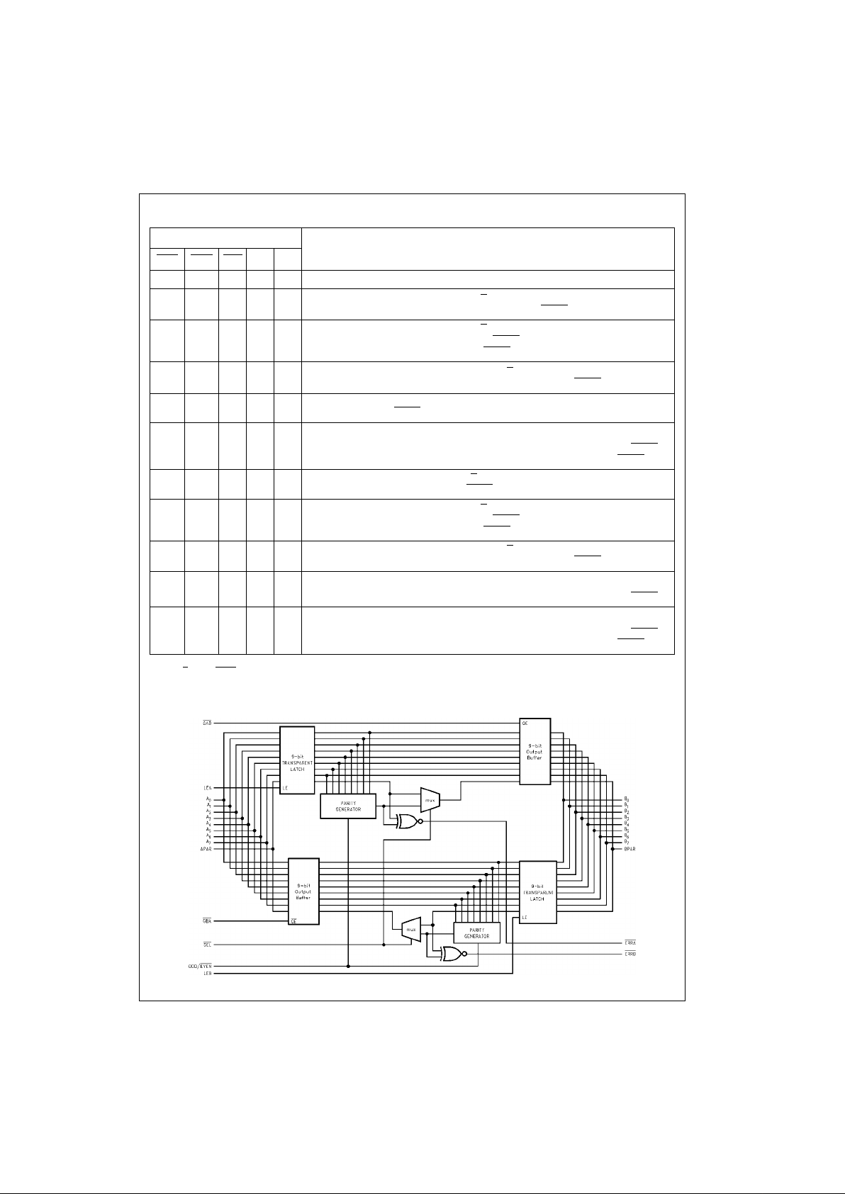
Function Table
H = HIGH Voltage Level L = LOW Voltage Level X = Immaterial
Note 1: O/E
= ODD/EVEN
Functional Block Diagram
Inputs
Operation
GAB
GBA SEL LEA LEB
H H X X X Busses A and B are 3-STATE.
HLLLH
Generates parity from B[0:7] based on O/E
(Note 1). Generated parity → APAR.
Generated parity checked against BPAR and output as ERRB
.
H L L H H Generates parity from B[0:7] based on O/E
. Generated parity → APAR. Generated
parity checked against BPAR and output as ERRB
. Generated parity also fed back
through the A latch for generate/check as ERRA
.
HLLXL
Generates parity from B latch data based on O/E
. Generated parity → APAR.
Generated parity checked against latched BPAR and output as ERRB
.
HLHXHBPAR/B[0:7] → APAR/A0:7] Feed-through mode. Generated parity checked against
BPAR and output as ERRB
.
H L H H H BPAR/B[0:7] → APAR/A[0:7]
Feed-through mode. Generated parity checked against BPAR and output as ERRB
.
Generated parity also fed back through the A latch for generate/check as ERRA
.
L H L H L Generates parity for A[0:7] based on O/E
. Generated parity → BPAR. Generated parity
checked against APAR and output as ERRA
.
L H L H H Generates parity from A[0:7] based on O/E
. Generated parity → BPAR. Generated
parity checked against APAR and output as ERRA
. Generated parity also fed back
through the B latch for generate/check as ERRB
.
L H L L X Generates parity from A latch data based on O/E
. Generated parity → BPAR.
Generated parity checked against latched APAR and output as ERRA
.
LHHHLAPAR/A[0:7] → BPAR/B[0:7]
Feed-through mode. Generated parity checked against APAR and output as ERRA
.
L H H H H APAR/A[0:7] → BPAR/B[0:7]
Feed-through mode. Generated parity checked against APAR and output as ERRA
.
Generated parity also fed back through the B latch for generate/check as ERRB
.

www.fairchildsemi.com 4
74F899
Absolute Maximum Ratings(Note 2) Recommended Operating
Conditions
Note 2: Absolute maximum ratings are values beyond which the device
may be damaged or have its useful life impaired. Functional operation
under these conditi ons is not implied.
Note 3: Either voltage limit or curren t limit is sufficient to protect in put s .
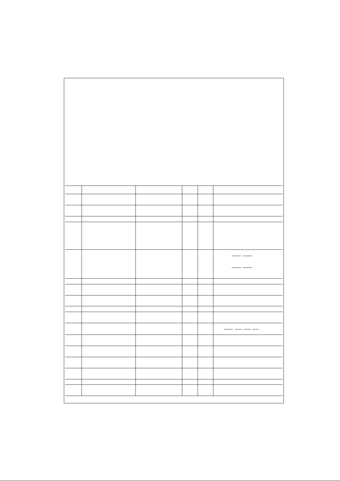
DC Electrical Characteristics
Storage Temperature −65°C to +150°C
Ambient Temperature under Bias −55°C to +125°C
Junction Temperature under Bias −55°C to +150°C
V
CC
Pin Potential to Ground Pin −0.5V to +7.0V
Input Voltage (Note 3) −0.5V to +7.0V
Input Current (Note 3) −30 mA to +5.0 mA
Voltage Applied to Output
in HIGH State (with V
CC
= 0V)
Standard Output −0.5V to V
CC
3-STATE Output −0.5V to +5.5V
Current Applied to Output
in LOW State (Max) Twice the Rated I
OL
(mA)
ESD Last Passing Voltage (Min) 4000V
Free Air Ambient Temperature 0°C to +70°C
Supply Voltage +4.5V to +5.5V
Symbol Parameter Min Typ Max Units
V
CC
Conditions
V
IH
Input HIGH Voltage 2.0 V Recognized as a
HIGH Signal
V
IL
Input LOW Voltage 0.8 V Recognized as a
LOW Signal
V
CD
Input Clamp Diode Voltage −1.2 V Min IIN = −18 mA
V
OH
Output HIGH 10% V
CC
2.5 IOH = −1 mA
Voltage 10% V
CC
2.4 IOH = −3 mA
10% V
CC
2.0 V IOH = −15 mA (Bn, BPAR)
5% V
CC
2.7 IOH = −1 mA
5% V
CC
2.7 IOH = −3 mA
V
OL
Output LOW 10% V
CC
0.5 IOL = 20 mA
Voltage
(An, APAR, ERRA, ERRB)
5% V
CC
0.55 V IOL = 24 mA
(An, APAR, ERRA, ERRB)
10% V
CC
0.55 IOL = 64 mA (Bn, BPAR)
V
TH
Input Threshold Voltage 1.45 V ±0.1V, Sweep Edge Rate must be > 1V/50 ns
V
OLV
Negative Ground Bounce
1.0 V
Observed on “quiet” output during
Voltage simultaneous switching of remaining outputs
V
OLP
Positive Ground Bounce
1.0 V
Observed on “quiet” output during
Voltage simultaneous switching of remaining outputs
I
IL
Input Low Current −0.6 mA Max VIN = 0.5V
I
IH
Input HIGH
5.0 µAMaxVIN = 2.7V
Current
I
BVI
Input HIGH Current
7.0 µAMax
VIN = 7.0V
Breakdown Test
(ODD/EVEN, GBA, GAB, SEL, LEA, LEB)
I
BVIT
Input HIGH Current
0.5 mA Max
VIN = 5.5V
Breakdown (I/O) (An, Bn, A
PAR
, B
PAR
)
I
CEX
Output HIGH
50 µAMaxV
OUT
= V
CC
Leakage Current
V
ID
Input Leakage
4.75 V 0.0
IID = 1.9 µA
Test All Other Pins Grounded
I
OD
Output Leakage
3.75 µA0.0
V
IOD
= 150 mV
Circuit Current All Other Pins Grounded
I
IL
Input Low Current −0.6 mA Max VIN = 0.5V
I
IH+
Output Leakage Current
70 µAMax
V
I/O
= 2.7V
I
OZH
Current (An, Bn, APAR, BPAR)
 Loading...