Fairchild Semiconductor 74F825SCX, 74F825SC, 74F825SPC Datasheet

© 1999 Fairchild Semiconductor Corporation DS009597 www.fairchildsemi.com
April 1988
Revised August 1999
74F825 8-Bit D-Type Flip-Flop
74F825
8-Bit D-Type Flip-Flop
General Description
The 74F825 is an 8-bit buffered register. It has Clock
Enable and Clear features which are ideal for parity bus
interfacing in high performance microprogramming systems. Also included in the 74F825 are multiple enables that
allow multi-user control of the interface.
Features
■ 3-STATE output
■ Clock enab le and clear
■ Multiple output enables
Ordering Code:
Devices also availab le in Tape and Reel. Specify by appending th e s uffix let t er “X” to the ordering code.
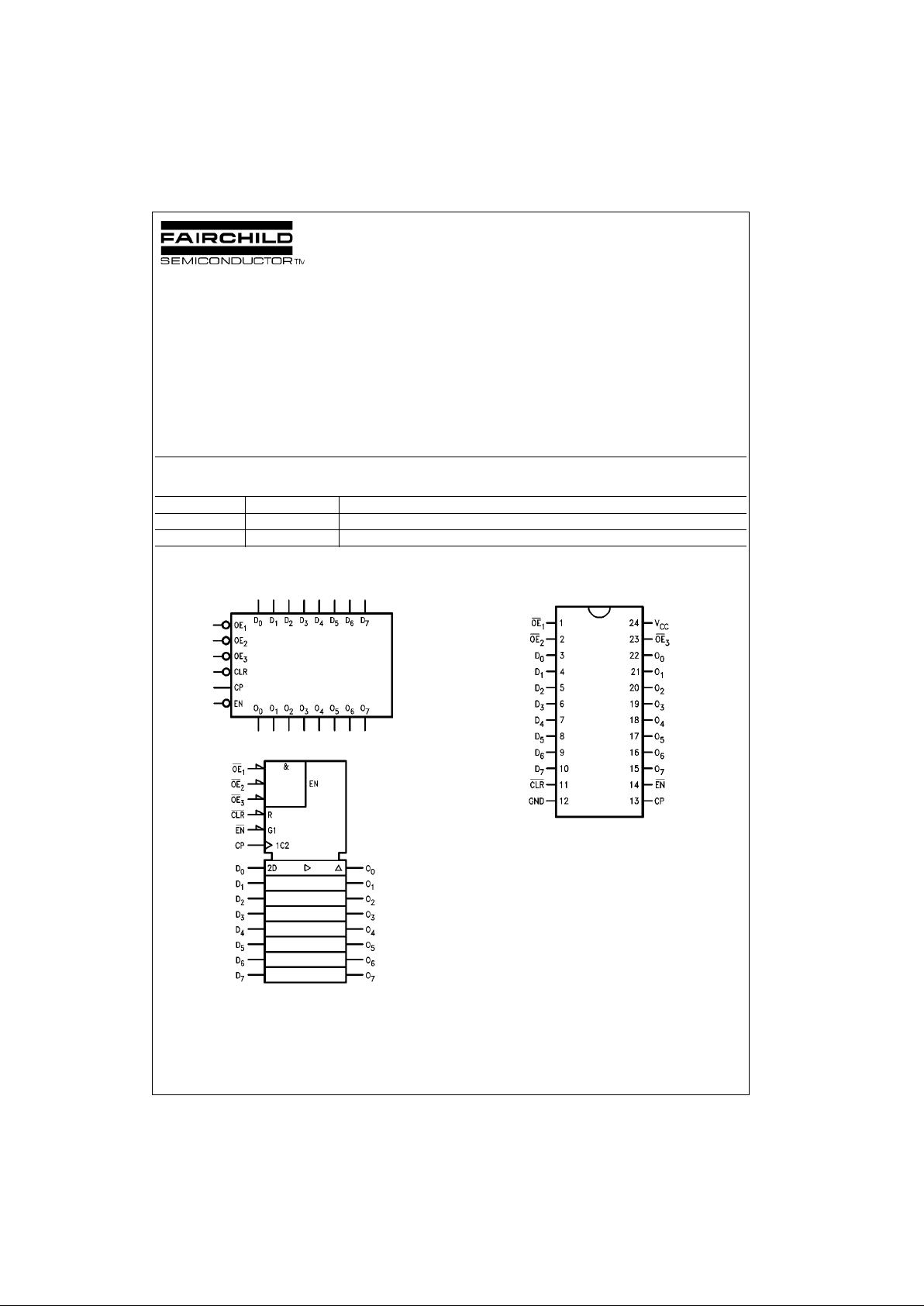
Logic Symbols
IEEE/IEC
Connection Diagram
Order Number Package Number Package Description
74F825SC M24B 24-Lead Small Outline Integrated Circuit (SOIC), JEDEC MS-013, 0.300 Wide
74F825SPC N24C 24-Lead Plastic Dual-In-Line Package (PDIP), JEDEC MS-100, 0.300 Wide

www.fairchildsemi.com 2
74F825
Unit Loading/Fan Out
Functional Description
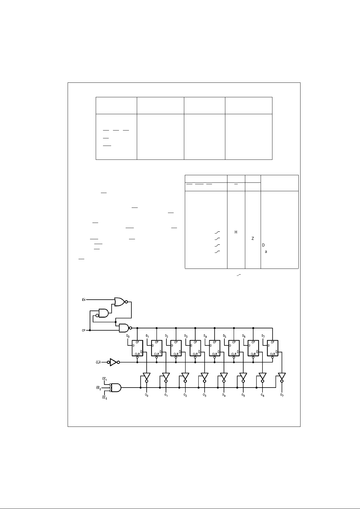
The 74F825 consis ts of eight D-type edge-triggered f lipflops. This device h as 3-STATE true outputs and is orga nized in broadside pinning. In addition to the clock and output enable pins, the buffered clock (CP) and buffered
Output Enable (OE
) are common to all flip-flops. The flipflops will store the state of their individual D inputs that
meet the setup and ho ld times requi rements on the L OWto-HIGH CP transition. With the OE
LOW the contents of
the flip-flops are av ailable at the outputs. W hen the OE
is
HIGH, the outputs go to th e high impeda nce state. Op eration of the OE
input does not affect t he state of the flip-
flops. The 74F825 has Clea r (CLR
) and Clock Enable (EN)
pins.
When the CLR
is LOW and the OE is LOW the outputs are
LOW. When CLR
is HIGH, data can be entered into the flip-
flops. When EN
is LOW, data on the inputs is transferred to
the outputs on the LOW-to-HIGH clock transition . When
the EN
is HIGH the outputs do not ch ange state, regard-
less of the data or clock input transitions.
Function Table
L = LOW Voltage Level Z = High Impedance
H = HIGH Voltage Level
= LOW-to-HIGH Transition
X = Immaterial NC = No Change
Logic Diagram
Please note that this diagram is provided o nly f or t he understanding of lo gic operations and should not be used to estimate propagation delays.
Pin Names Description
U.L.
Input I
IH/IIL
HIGH/LOW
Output I
OH/IOL
D0–D
7
Data Inputs 1.0/1.0 20 µA/−0.6 mA
O
0–O7
3-STATE Data Outputs 150/40 (33.3) −3 mA/24 mA (20 mA)
OE
1
, OE2, OE
3
Output Enable Input 1.0/1.0 20 µA/−0.6 mA
EN
Clock Enable 1.0/1.0 20 µA/−0.6 mA
CLR
Clear 1.0/1.0 20 µA/−0.6 mA
CP Clock Input 1.0/2.0 20 µA/−1.2 mA
Inputs Internal Output
Function
OE
CLR EN CP D Q O
HHLHXNC ZHold
HHLLXNC ZHold
H H H X X NC Z Hold
LHHXXNC NCHold
H L X X X H Z Clear
L L X X X H L Clear
HHL
L H Z Load
HHL
H L Z Load
LHL
L H L Data Available
LHL
H L H Data Available
L H L H X NC NC No Change in Data
L H L L X NC NC No Change in Data
 Loading...