

Fairchild Semiconductor 74F794SCX, 74F794SC, 74F794PC Datasheet
© 1999 Fairchild Semiconductor Corporation DS010652 www.fairchildsemi.com
March 1990
Revised August 1999
74F794 8-Bit Register with Readback
74F794
8-Bit Register with Readback
General Description
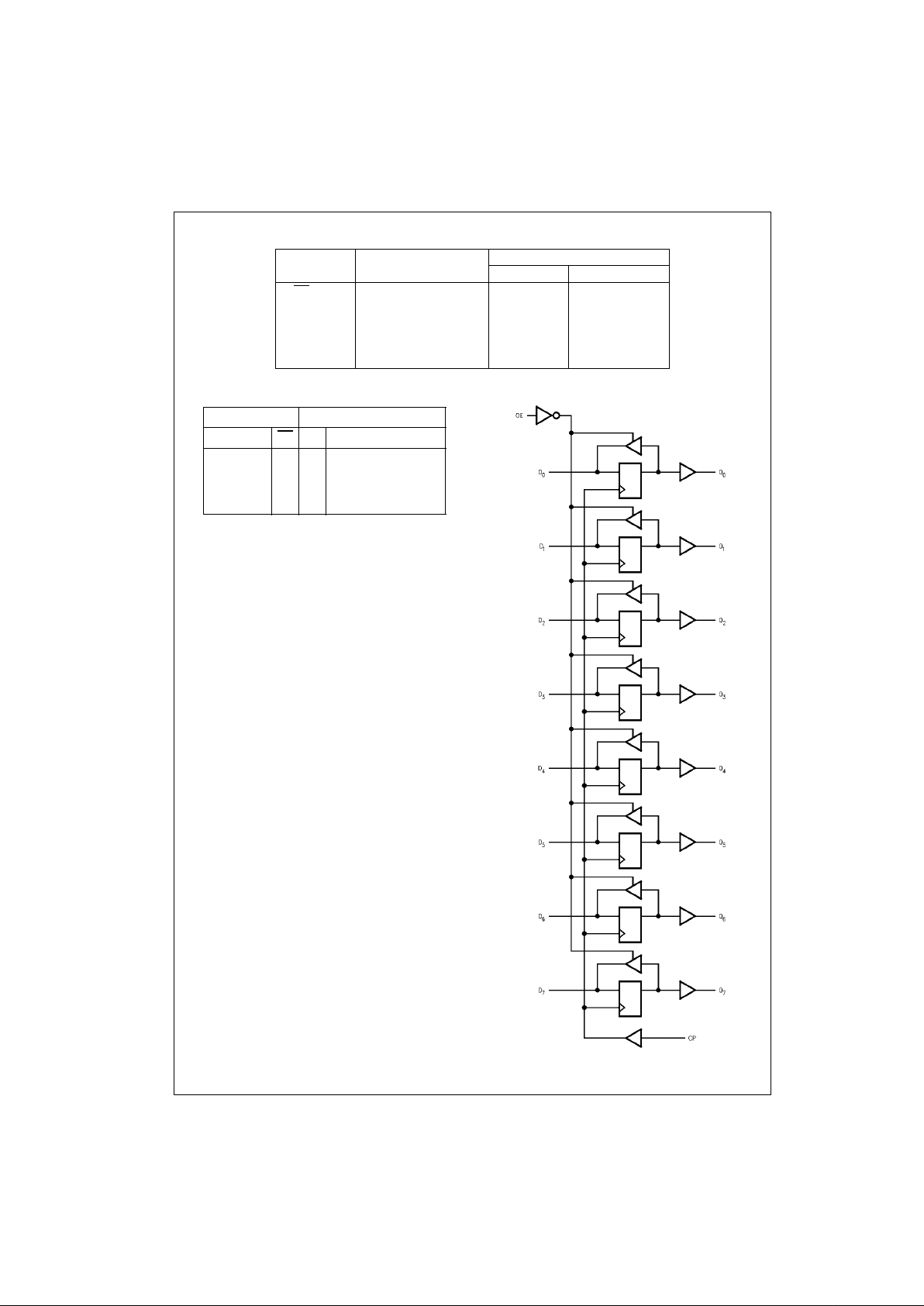
The 74F794 is an 8-bit register with readback capability
designed to store data as well as read the register information back onto the data bus. The I/O bus (D bus) has 3STATE outputs. Current sinking capability is 64 mA on both
the D and Q busses.
Data is loaded into the registers on the LOW-to-HIGH transition of the clock (CP). The outp ut enable (OE
) is used to
enable data on D
0–D7
. When OE is LOW, the output of the
registers is enabled on D
0–D7
, enabling D as an outp ut
bus. When OE is HIGH, D
0–D7
are inputs to t he registers
configuring D as an input bus.
Features
■ 3-STATE outputs on the I/O port
■ D and Q output sink capability of 64 mA
■ Functionally and pin equivalent to the 74LS794
Ordering Code:
Devices also availab le in Tape and Reel. Specify by appending th e s uffix let t er “X” to the ordering code.
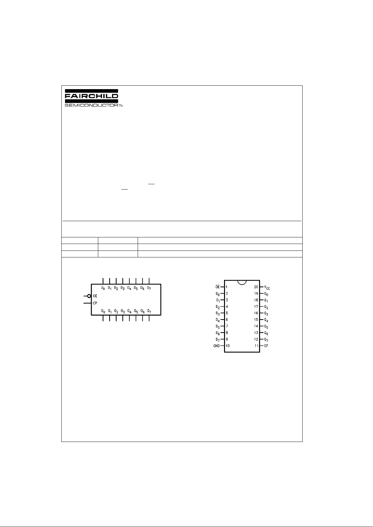
Logic Symbol Connection Diagram
Order Number Package Number Package Description
74F794SC M20B 20-Lead Small Outline Integrated Circuit (SOIC), JEDEC MS-013, 0.300 Wide
74F794PC N20A 20-Lead Plastic Dual-In-Line Package (PDIP), JEDEC MS-001, 0.300 Wide
www.fairchildsemi.com 2
74F794
Input Loading/Fan-Out
Truth Table
Note 1: In this case the output of the regi ster is clocked t o the inputs an d
the overall Q output is unc hanged at Q
n
.
Logic Diagram
Pin Names Description
HIGH/LOW
(U.L.) Current
OE
Output Enable Input 1.0/1.0 20 µA/−0.6 mA
CP Clock Pulse Inputs 1.0/1.0 20 µA/−0.6 mA
D
0–D7
D Bus Inputs/ 3.5/1.083 70 µA/−650 µA
3-STATE Outputs 750/106.6 −15 mA/64 mA
Q
0–Q7
Q Bus Outputs 750/106.6 −15 mA/64 mA
Inputs Outputs
CP OE
QD
L or H or ↓ LQ
n
Output, Q
L or H or ↓ HQ
n
Input
↑ LQ
n
Output, Q (Note 1)
↑ H D Input
 Loading...