

Fairchild Semiconductor 74F676SPC, 74F676SCX, 74F676SC, 74F676PC Datasheet
© 1999 Fairchild Semiconductor Corporation DS009588 www.fairchildsemi.com
April 1988
Revised August 1999
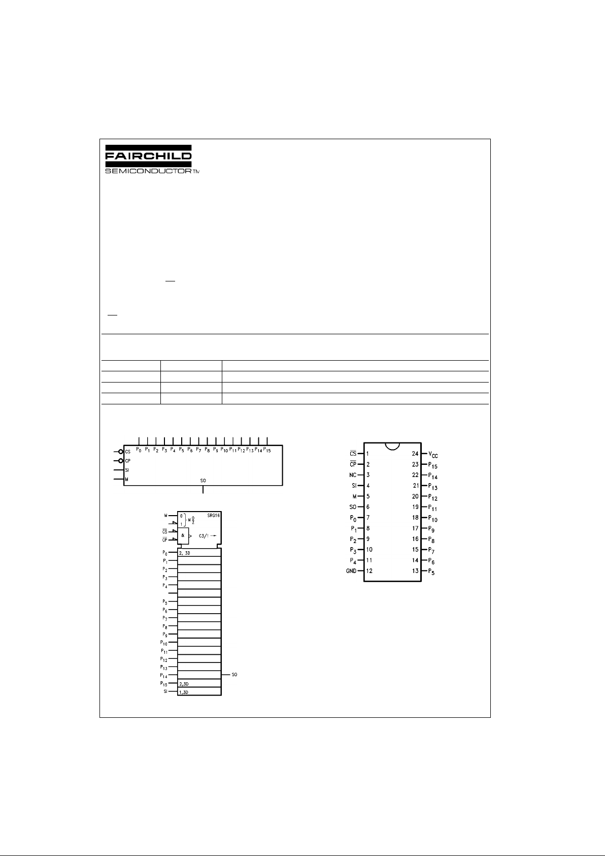
74F676 16-Bit Serial/Parallel-In, Serial-Out Shift Register
74F676
16-Bit Serial/Parallel-In, Serial-Out Shift Register
General Description
The 74F676 contains 16 fl ip-flops with provision for synchronous parallel or serial entry and serial output . When
the Mode (M) input is HIGH, information present on the
parallel data (P
0–P15
) inputs is entered on the falling edge
of the Clock Pulse (CP
) input signal. When M is LOW, data
is shifted out of the most significant bit p osition while info rmation present on the Ser ial (SI) input shi fts into the le ast
significant bit position. A H IGH signal on the Chip Select
(CS
) input prevents both parallel and serial operations.
Features
■ 16-bit parallel-to-serial conversion
■ 16-bit serial-in, serial-out
■ Chip select control
■ Slim 24 lead 300 mil package
Ordering Code:
Devices also availab le in Tape and Reel. Specify by appending th e s uffix let t er “X” to the ordering code.
Logic Symbols
IEEE/IEC
Connection Diagram
Order Number Package Number Package Description
74F676SC M24B 28-Lead Small Outline Integrated Circuit (SOIC), JEDEC MS-013, 0.300 Wide
74F676PC N24A 24-Lead Plastic Dual-In-Line Package (PDIP), JEDEC MS-010, 0.600 Wide
74F676SPC N24C 24-Lead Plastic Dual-In-Line Package (PDIP), JEDEC MS-100, 0.300 Wide
www.fairchildsemi.com 2
74F676
Unit Loading/Fan Out
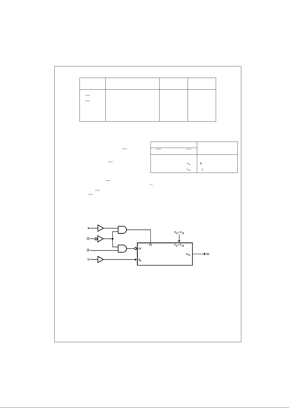
Functional Description
The 16-bit shift register o per ate s in one of thr ee m ode s, as
indicated in the Shift Register Operations Table.
HOLD— a HIGH signal on the Ch ip Select ( CS
) input pre-
vents clocking, and data is stored in the sixteen registers.
Shift/Serial Load— data present on the SI pin shifts into
the register on the falling edge of CP
. Data enters the Q
0
position and shifts toward Q15 on successive clocks, finally
appearing on the SO pin.
Parallel Load— data present on P
0–P15
are entered into
the register on the falling edge of CP
. The SO output repre-
sents the Q
15
register output.
To prevent false cloc king, CP
must be LOW during a LOW-
to-HIGH transition of CS
.
Shift Register Operations Table
H = HIGH Voltage Level
L = LOW Voltage Level
X = Immaterial
= HIGH-to-LOW Tran s iti on
Block Diagram
Pin Names Description
U.L.
Input I
IH/IIL
HIGH/LOW
Output I
OH/IOL
P0–P
15
Parallel Data Inputs 1.0/1.0 20 µA/−0.6 mA
CS
Chip Select Input (Active LOW) 1.0/1.0 20 µA/−0.6 mA
CP
Clock Pulse Input (Active LOW) 1.0/1.0 20 µA/−0.6 mA
M Mode Select Input 1.0/1.0 20 µA/−0.6 mA
SI Serial Data Input 1.0/1.0 20 µA/−0.6 mA
SO Serial Output 50/33.3 −1 mA/20 mA
Control Input
Operating Mode
CS
MCP
HXXHold
LL
Shift/Serial Load
LH
Parallel Load
 Loading...