

Fairchild Semiconductor 74F675ASPC, 74F675ASCX, 74F675ASC, 74F675APC Datasheet

© 1999 Fairchild Semiconductor Corporation DS009587 www.fairchildsemi.com
April 1988
Revised August 1999
74F675A 16-Bit Serial-In, Serial/Parallel-Out Shift Register
74F675A
16-Bit Serial-In, Serial/Parallel-Out Shift Register
General Description
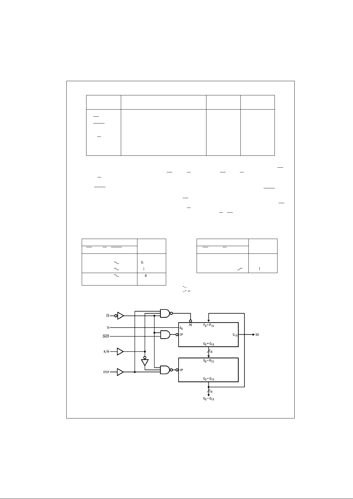
The 74F675A contai ns a 16 -b it ser ial in/ seri a l out shift register and a 16-bit parallel out storage register. Separate
serial input and output pins are provided for expansio n to
longer words. By me ans of a sep arate clock, the contents
of the shift register are transferred to the storage register.
The contents of th e storage register can also be lo aded
back into the shift register. A HIGH signal on the Chip
Select input prevents both shifting and parallel loading.
Features
■ Serial-to-parallel converter
■ 16-Bit serial I/O shift register
■ 16-Bit parallel out storage register
■ Recirculating parallel transfer
■ Expandable for longer word s
■ Slim 24 lead package
■ 74F675A version prevents false clocking through
CS
or R/W inputs
Ordering Code:
Devices also availab le in Tape and Reel. Specify by appending th e s uffix let t er “X” to the ordering code.
Logic Symbols
IEEE/IEC
Connection Diagram
Order Number Package Number Package Description
74F675ASC M24B 24-Lead Small Outline Integrated Circuit (SOIC), JEDEC MS-013, 0.300 Wide
74F675APC N24A 24-Lead Plastic Dual-In-Line Package (PDIP), JEDEC MS-010, 0.600 Wide
74F675ASPC N24C 24-Lead Plastic Dual-In-Line Package (PDIP), JEDEC MS-100, 0.300 Wide
www.fairchildsemi.com 2
74F675A
Unit Loading/Fan Out
Functional Description
The 16-Bit shift register op erates in one of fou r modes, as
determined by t he sign als applied to th e Chip S elect ( CS
),
Read/Write (R/W
) and Store Clock Pulse (STCP) input.
State changes are indi ca ted by the fa l ling edg e of the Shift
Clock Pulse (SHCP
). In the Shift Right mode , data enters
D
0
from the Serial Input (S I) pin and exits f rom Q15 via the
Serial Data Output (SO) pin. In the Parallel Load mode,
data from the storage re gister out puts ent er the shi ft reg ister and serial shifting is inhibited.
The storage register is in the Hold mode when either CS
or
R/W
is HIGH. With CS and R/W both LOW, the storage
register is parallel loaded fro m the shift registe r on the rising edge of STCP.
To prevent false clocking of the shift register, SHCP
should
be in the LOW state during a LOW-to-HIGH transition of
CS
. To prevent false clocking of the storage register, STCP
should be LOW during a HIGH-to-LOW transition of CS
if
R/W
is LOW, and should also be LOW during a HIGH-to-
LOW transition of R/W
if CS is LOW.
Shift Register Operations Table Storage Register Operations Table
H = HIGH Voltage Level
L = LOW Voltage Level
X = Immaterial
= HIGH-to-LOW Tran s iti on
= LOW-to-HIGH Transition
Logic Diagram
Please note that this diagram is provided o nly f or t he understanding of lo gic operations and should not be used to estimate propagation delays.
Pin Names Description
U.L.
Input I
IH/IIL
HIGH/LOW
Output I
OH/IOL
SI Serial Data Input 1.0/1.0 20 µA/−0.6 mA
CS
Chip Select Input (Active LOW) 1.0/1.0 20 µA/−0.6 mA
SHCP
Shift Clock Pulse Input (Active Falling Edge) 1.0/1.0 20 µA/−0.6 mA
STCP Store Clock Pulse Input (Active Rising Edge) 1.0/1.0 20 µA/−0.6 mA
R/W
Read/Write Input 1.0/1.0 20 µA/−0.6 mA
SO Serial Data Output 50/33.3 −1 mA/20 mA
Q
0–Q15
Parallel Data Outputs 50/33.3 −1 mA/20 mA
Control Inputs Operating
CS
R/W SHCP STCP Mode
H X X X Hold
LL
X Shift Right
LH
L Shift Right
LH
H Par all el Loa d,
No Shifting
Inputs Operating
CS
R/W STCP Mode
HXXHold
LHXHold
LL
Parallel Load
 Loading...