

Fairchild Semiconductor 74F657SPC, 74F657SCX, 74F657SC Datasheet
© 1999 Fairchild Semiconductor Corporation DS009584 www.fairchildsemi.com
March 1988
Revised August 1999
74F657 Octal Bidirectional Transceiver with
74F657
Octal Bidirectional Transceiver with
8-Bit Parity Generator/Checker and 3-STATE Outputs
General Description
The 74F657 contains eight non-inverting buffers with 3STATE outputs and an 8-bi t parity genera tor/checker. It is
intended for bus-oriented applications. The buffers have a
guaranteed current sinking capability of 24 mA at the A
Port and 64 mA at the B Port.
Features
■ 300 Mil 24-pin slimline DIP
■ Combines 74F245 and 74F280A functions in one
package
■ 3-STATE outputs
■ B Outputs sink 64 mA
■ 12 mA source current, B side
■ Input diodes for termination effects
Ordering Code:
Devices also availab le in Tape and Reel. Specify by appending th e s uffix let t er “X” to the ordering code.
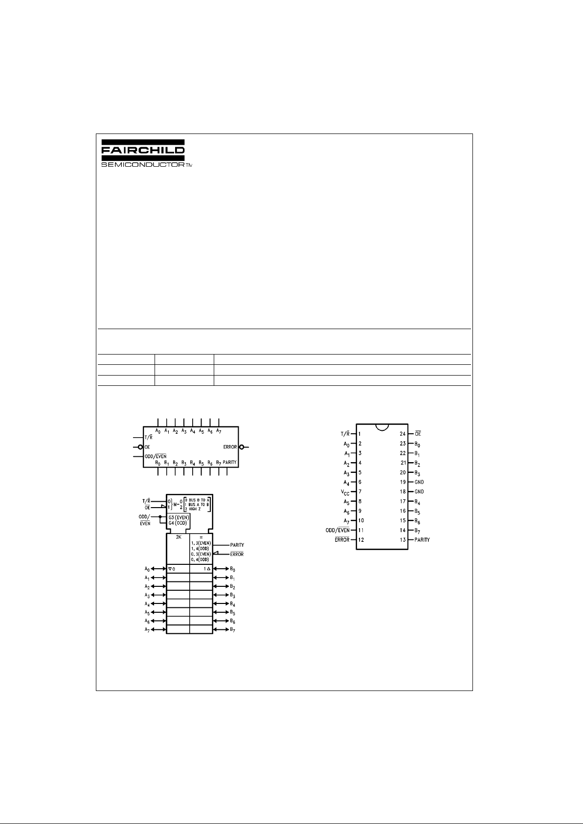
Logic Symbols
IEEE/IEC
Connection Diagram
Order Number Package Number Package Description
75F657SC M24B 24-Lead Small Outline Integrated Circuit (SOIC), JEDEC MS-013, 0.300 Wide
74F657SPC N24C 24-Lead Plastic Dual-In-Line Package (PDIP), JEDEC MS-100, 0.300 Wide
www.fairchildsemi.com 2
74F657
Unit Loading/Fan Out
Functional Description
The Transmit/Receive (T/R) input determines the direction
of the data flow through the bidirectional transceivers.
Transmit (active HIGH) enables data from the A Port to the
B Port; Receive (active LOW) enables data from the B Port
to the A Port.
The Output Enable (OE
) input disables the parity and
ERROR
outputs and both the A and B Ports by pl acing
them in a HIGH-Z co ndition when the O utput En able input
is HIGH.
When transmitting (T/R
HIGH), the parity generator detects
whether an even or odd numbe r of bits on the A Port ar e
HIGH and compares these wi th the condition of the pa rity
select (ODD/EVEN
). If the Parity Select is HIGH and an
even number of A inputs are HIGH, the Parity output is
HIGH.
In receiving mode (T/R
LOW), the parity select and number
of HIGH inputs on port B a re compar ed to the condi tion of
the Parity input. If an even number of bits on the B Port are
HIGH, the parity select is HIGH, and the PARITY input is
HIGH, then ERROR
will be HIGH to indicate no error. If an
odd number of bits on the B Port are HIGH, the parity
select is HIGH, and the PARITY input is HIGH, the ERROR
will be LOW indicating an error.
Function Table
H = HIGH Voltage Level
L = LOW Voltage Level
X = Immaterial
Z = High Impedance
Function Table
H = HIGH Voltage Level
L = LOW Voltage Level
X = Immaterial
Pin Names Description
U.L.
Input I
IH/IIL
HIGH/LOW
Output I
OH/IOL
A0–A
7
Data Inputs/ 4.5/0.15 90 µA/− 90 µA
3-STATE Outputs 150/40 (33.3) −3 mA/24 mA (20 mA)
B
0–B7
Data Inputs/ 3.5/0.117 70 µA/−70 µA
3-STATE Outputs 600/106.6 (80) −12 mA/64 mA (48 mA)
T/R
Transmit/Receive Input 2.0/0.067 40 µA/−40 µA
OE
Enable Input 2.0/0.067 40 µA/−40 µA
PARITY Parity Input/ 3.5/0.117 70 µA/−70µA
3-STATE Output 600/106.6 (80) −12 mA/64 mA (48 mA)
ODD/EVEN
ODD/EVEN Parity Input 1.0/0.033 20 µA/−20 µA
ERROR
Error Output 600/106.6 (80) −12 mA/64 mA (48 mA)
Number of
Inputs that
are HIGH
Inputs
Input/
Outputs
Output
OE
T/R
ODD/
Parity ERROR
Outputs
EVEN
Mode
0, 2, 4, 6, 8 L H H H Z Transmit
LH L L Z Transmit
LL H H H Receive
LL H L L Receive
LL L H L Receive
LL L L H Receive
1, 3, 5, 7 L H H L Z Transmit
LH L H Z Transmit
LL H H L Receive
LL H L H Receive
LL L H H Receive
LL L L L Receive
Immaterial H X X Z Z Z
Inputs
Outputs
OE
T/R
L L Bus B Data to Bus A
L H Bus A Data to Bus B
H X High-Z State
3 www.fairchildsemi.com
74F657
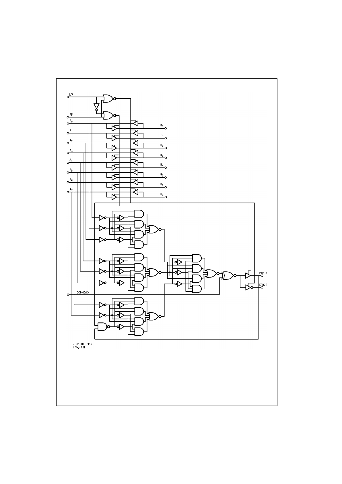
Functional Block Diagram
 Loading...